Info snack: Alder Lake-M + Raptor Lake-S layout (Mockup)
On today’s agenda, we will quickly cover two topics.
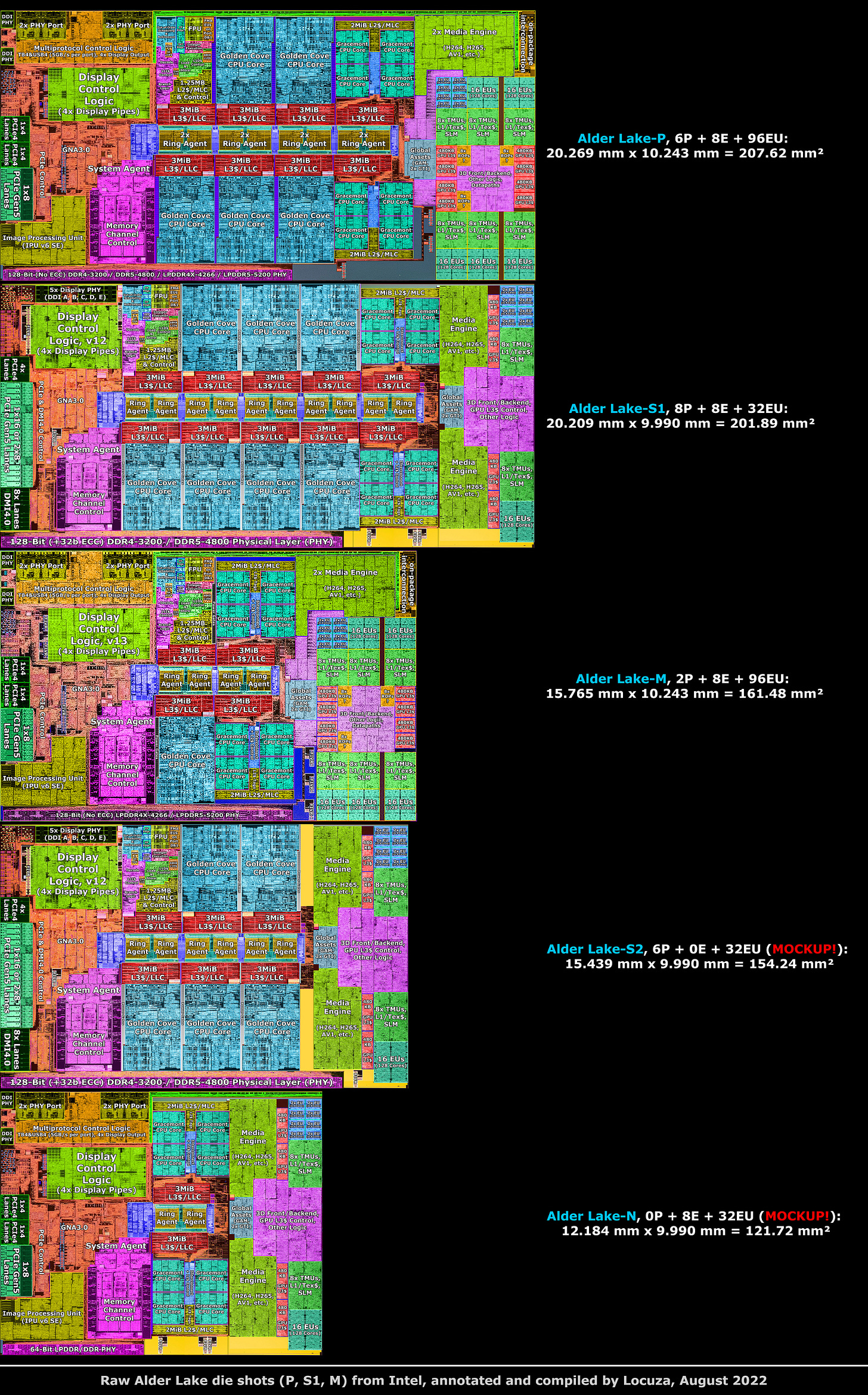
1. A small overview of all Alder Lake chips, including a real die shot of Alder Lake-M (2P + 6E + 96EU).
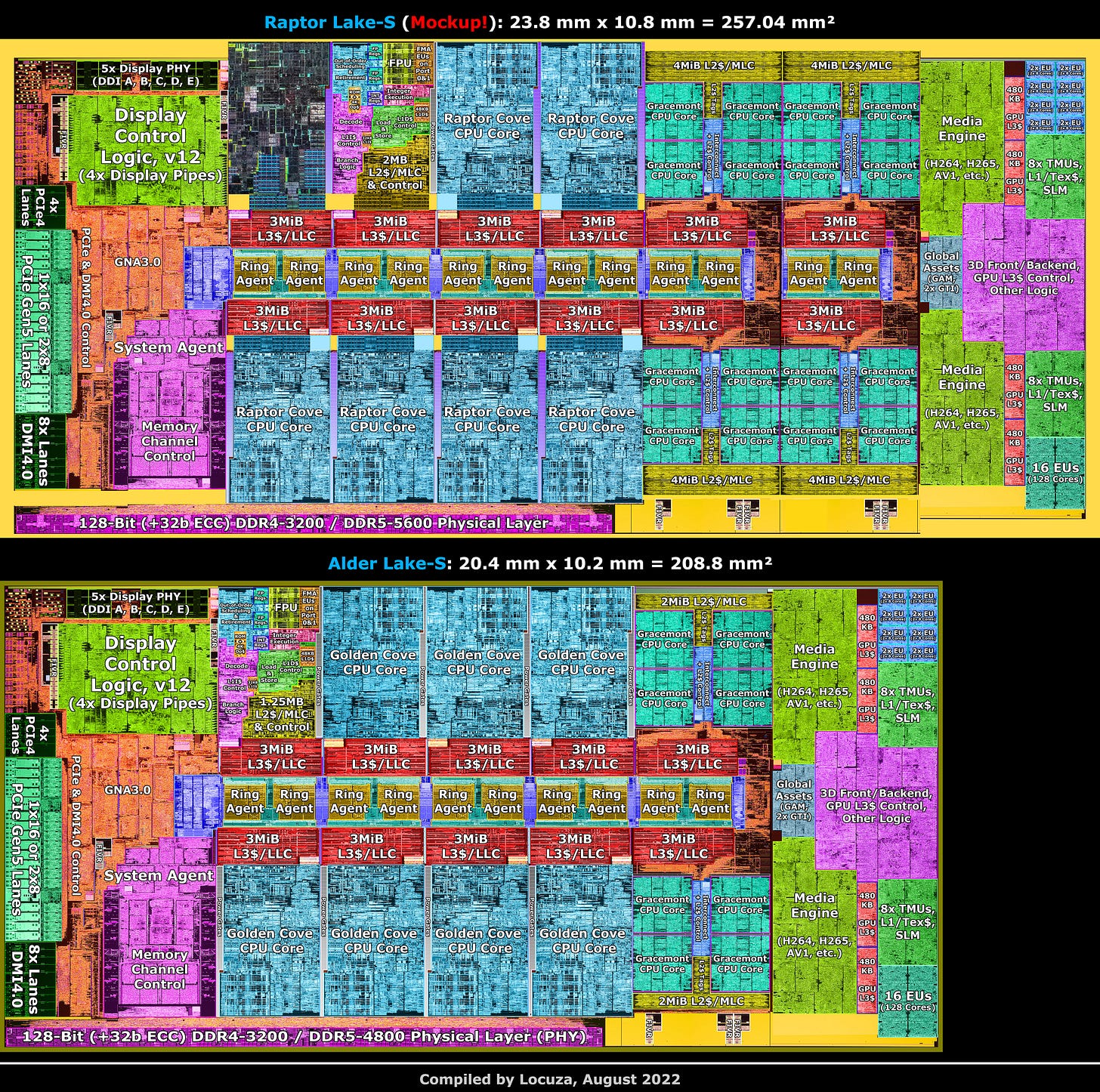
2. A speculative look at the upcoming Raptor Lake-S layout (8P + 16E + 32EU).
1. Alder Lake
1.1. Let's start with a neat info.
In the last Alder Lake walkthrough, the question was raised why the iGPU blocks of Alder Lake-S are much larger than previously on Tiger Lake or the Alder Lake-P chip? Intel did not increase the product clock rates by any significant amount, and with a high-density implementation they could have made the chip smaller and/or include extra redundancies to improve yields.
To my surprise, Raja Koduri (Executive Vice President of AXG at Intel) replied:

The main reason for using larger cells was yield.
I hadn't thought of that option, but in hindsight it sounds logical that larger cells would suffer fewer manufacturing errors than smaller, densely packed cells.
It should be easier, design wise, to reimplement the blueprint with larger cells than to add more redundant structures.
1.2. Last time we went over the differences between Alder Lake-S and -P, and now we can check out Alder Lake-M!
Compared to ADL-S (8P) and ADL-P (6P), the CPU engine only has 2 P cores, but keeps 8 E-Cores around.
Two major attributes are shared with ADL-P, namely an iGPU with 96 EUs and an integrated IPU (Image Processing Unit).
For those components, one would expect 1:1 reuse.
In comparison to the ADL-P chip, two cut-downs happened, spec wise.
Instead of 4x Thunderbolt 4 ports, only 2x ports are available.
Furthermore, only 4x PCIe Gen4 lanes are going out to an SSD, instead of possibly 2x4 for two devices and no PCIe lanes are provided for discrete GPU usage.
Lastly, the platform can only handle LPDDR4X or LPDDR5 memory, DDR standards are not supported and ECC (Error Correction Code) is missing as in ADL-P.
So by and large one would expect ADL-M to look very similar to ADL-P, with perhaps a smaller uncore area, as only 4x PCIe4 lanes and 2x TB4 ports are provided.
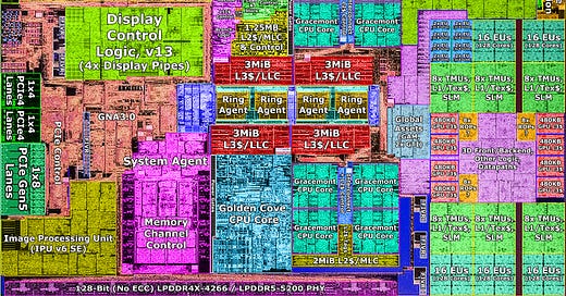
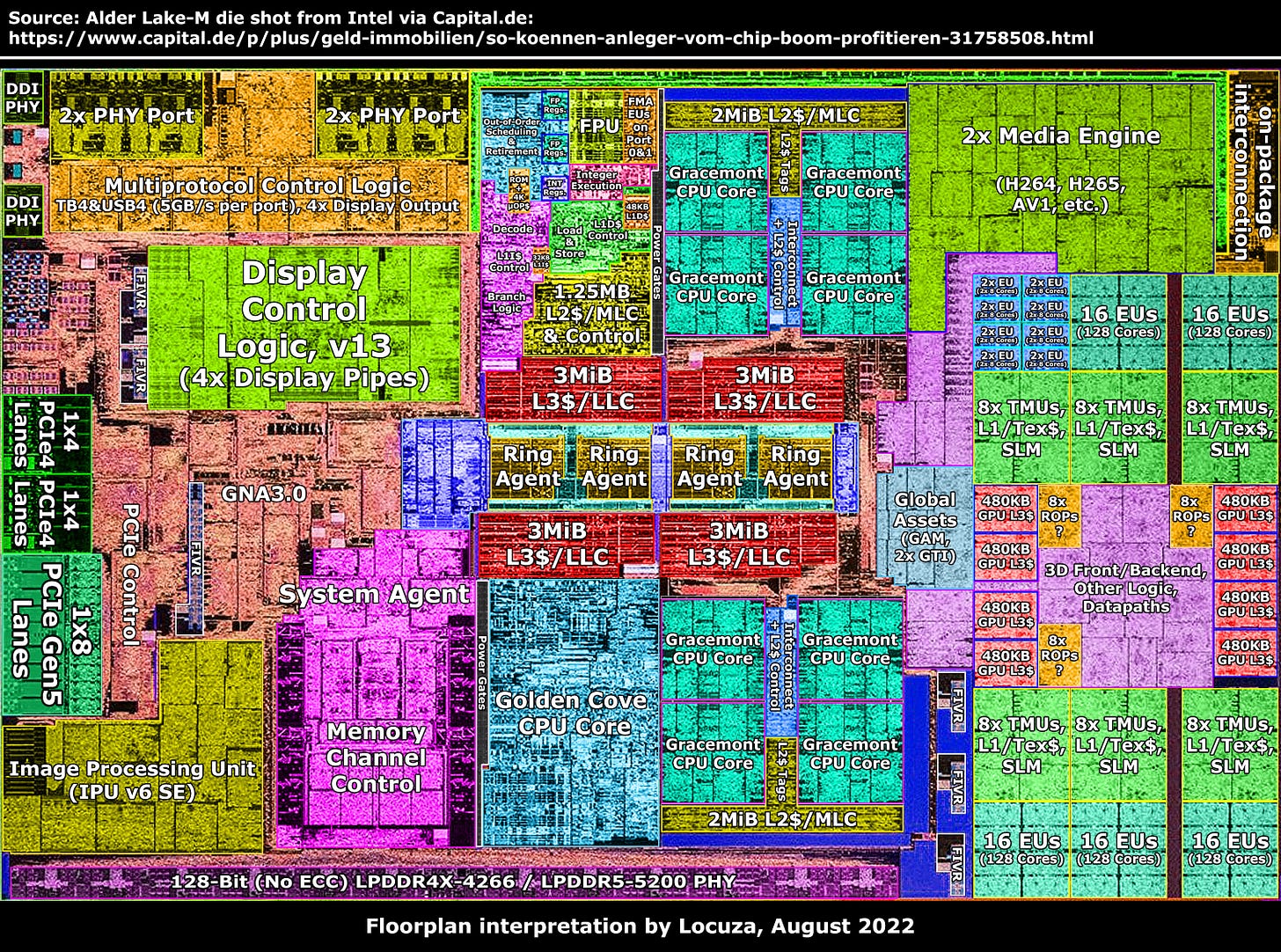
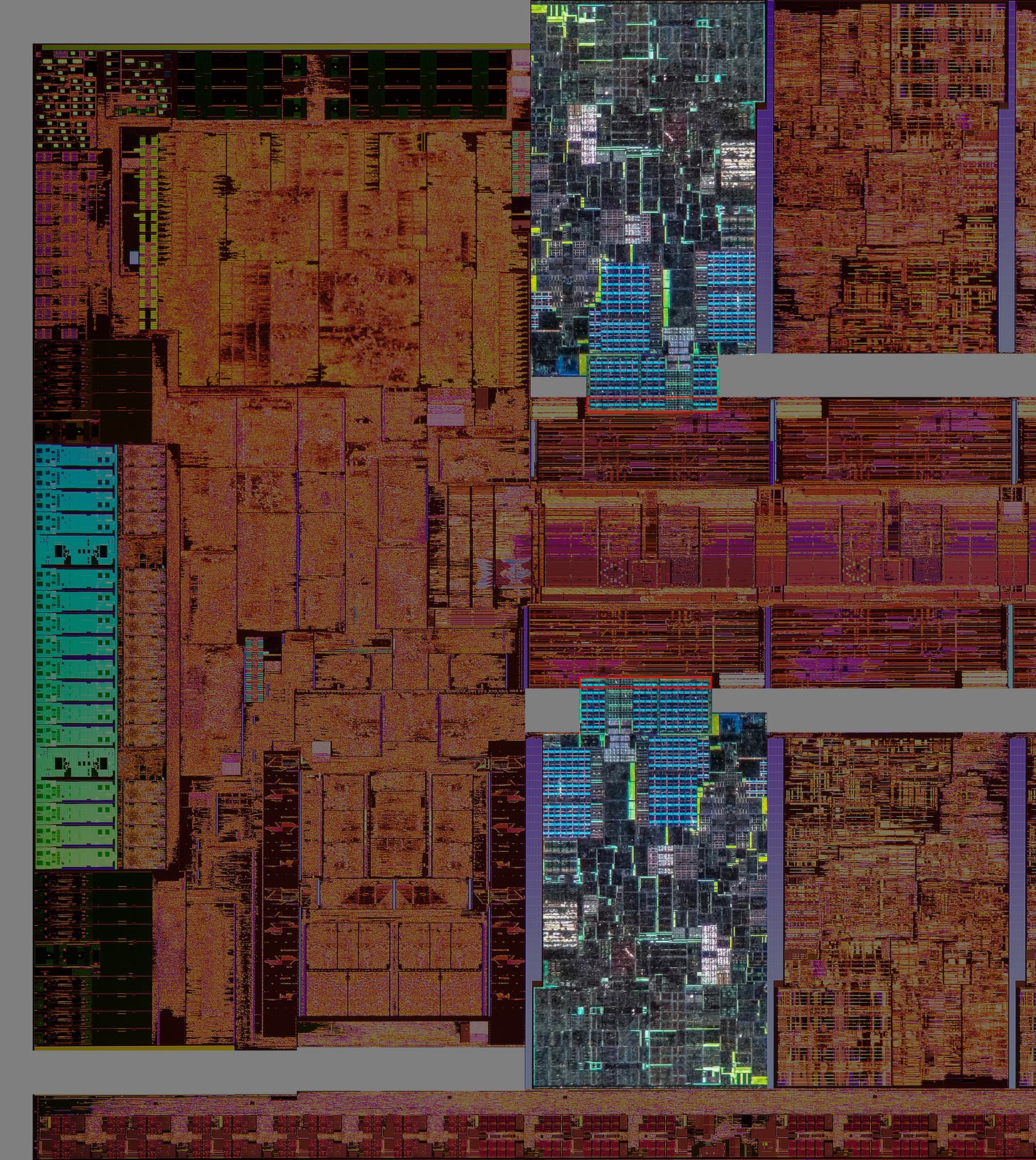
Quite amazingly and by sheer coincidence, cha0shacker found an ADL-M die shot from Intel on Capital.de:

And…, drum roll, the chip looks nearly identical to the ADL-P design.
Physically, the same 4x TB4 complex is present, together with 2x 4-Lane PCIe4 and 1x 8-Lane PCIe5 PHYs.
Thus, the product limitations are not chip based.
There are really only two small differences. The interconnection path from the on-package interconnect (OPI) to the System Agent complex is just shorter and one DDR FIVR (Fully Integrated Voltage Regulator) is now closer located to the PHY, directly below the FIVRs for the E-Core L2 Cache.
1.3. There is another dedicated Alder Lake chip that we know of, but are missing a die shot off (with visible structures).
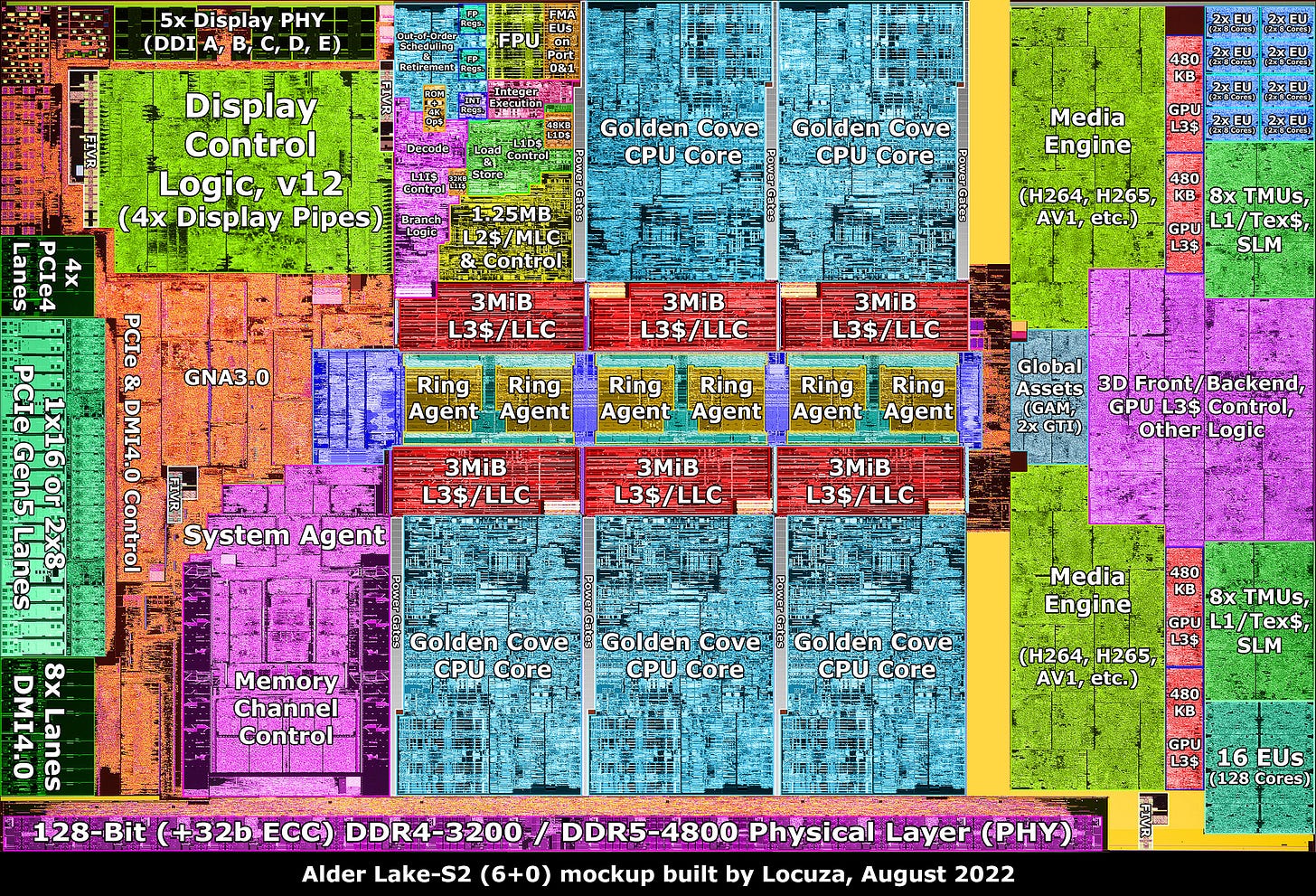
It's Alder Lake-S2*, a smaller S-die that comes with 6 P-Cores and no E-Cores at all. While we don’t have a die shot with exposed features, we do have a chip+ package photo, which reveals the whole die size:
https://videocardz.com/newz/msi-confirms-there-are-two-die-variants-of-alder-lake-s-desktop-cpus
Similar to Alder Lake-M, S2 should reuse almost everything from the S1* chip layout. So a mockup can be quickly built:
* S"1" and S"2" are freely chosen designations for the 8P+8E chip, respectively the 6P+0E die.
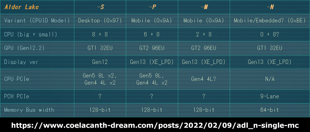
1.4. There is (maybe) also a fifth Alder Lake chip, Alder Lake-N.
The software entries for it are quite interesting:
https://www.coelacanth-dream.com/posts/2022/02/09/adl_n-single-mc https://www.coelacanth-dream.com/posts/2022/01/12/adl_n-chromebook-board/ https://www.coelacanth-dream.com/posts/2021/11/25/adl_n-atom-only/
1. There are no P-Cores at all, only 8 E-Cores are available.
This is unique as Intel does not allow all P-Cores to be disabled on currently available Alder Lake chips as at least one P-Core is required to load the boot firmware.
2. The iGPU has 32 EUs (same high-performance implementation as on ADL-S?)
3. The Display IP is v13 as in ADL-P and not v12 as in ADL-S chips.
4. There are 2x Thunderbolt 4 / Type-C ports, as in ADL-M, however physically one might see again the same 4x TB4 complex.
5. Only one memory controller is said to be present and 64b going out to memory.
6. There are no PCIe lanes coming out of the SoC.
In regard to the die size, a lot depends on how much Intel reused and what they decided to redesign.
Did they really remove the PCIe PHYs, one Memory Controller, are they using the same CPU cache sizes, and so on?
The simplest mockup, with maximum reuse, would look like this:
1.5 All Alder Lake chips next to each other, from the largest (P-die) to the smallest (N-die) chip (without scribe lines):
2. Raptor Lake-S
Currently, it’s assumed that Intel will reveal Raptor Lake (RPL) in more detail at the Intel Innovation event on September 27-28.
According to rumors, AMD decided to delay their Zen 4 Raphael (RPL) sale launch to the same date, potentially to also directly annoy Intel (besides firmware issues).
We look forward to this repartee, because after all there can be only one RPL (*windows shattering*).
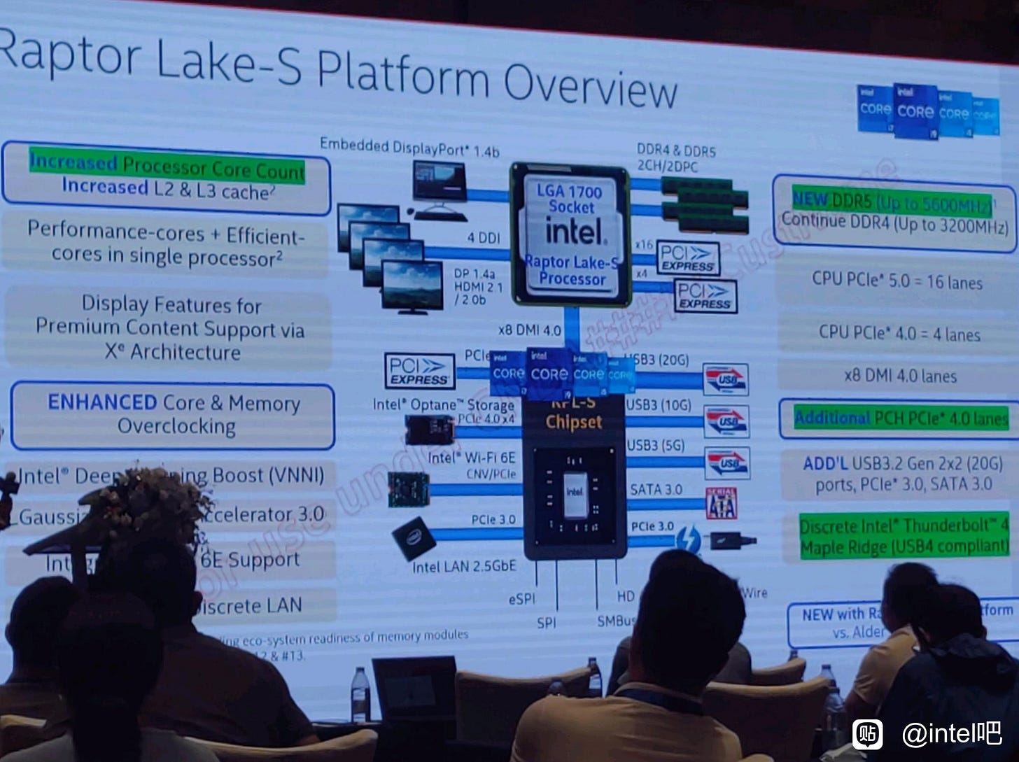
What Intel will bring to the table has been outlined by legitimate leaks for many months. Raptor Lake will use Raptor Cove (P-Core), whose architecture appears to be largely identical to Golden Cove in Alder Lake.
A key change is the L2 cache capacity, which grows from 1.25 MB to 2 MB, the same capacity as the Golden Cove server variant.
The access latency will likely also get worse by one cycle from 15 to 16.
In addition, it's claimed that frontend and last-level cache improvements have been done (to be seen).
Contrary to Raptor Cove, the E-Cores are still named Gracement, but their shared L2 cache is also getting larger.
From 2 MB it’s doubled to 4 MB.
Moreover, the Raptor Lake-S chip will include two additional E-Core clusters, pumping up the (main) core number to 24 (8P + 16E).
Another addition, at least for the mobile segment, will be the usage of a DLVR (Digital Linear Voltage Regulator) system. The DLVR can significantly reduce the voltage input levels, but the benefit is quickly decreasing after a certain current strenght, which could be the reason why a marketing slide did not state it for the desktop segment.
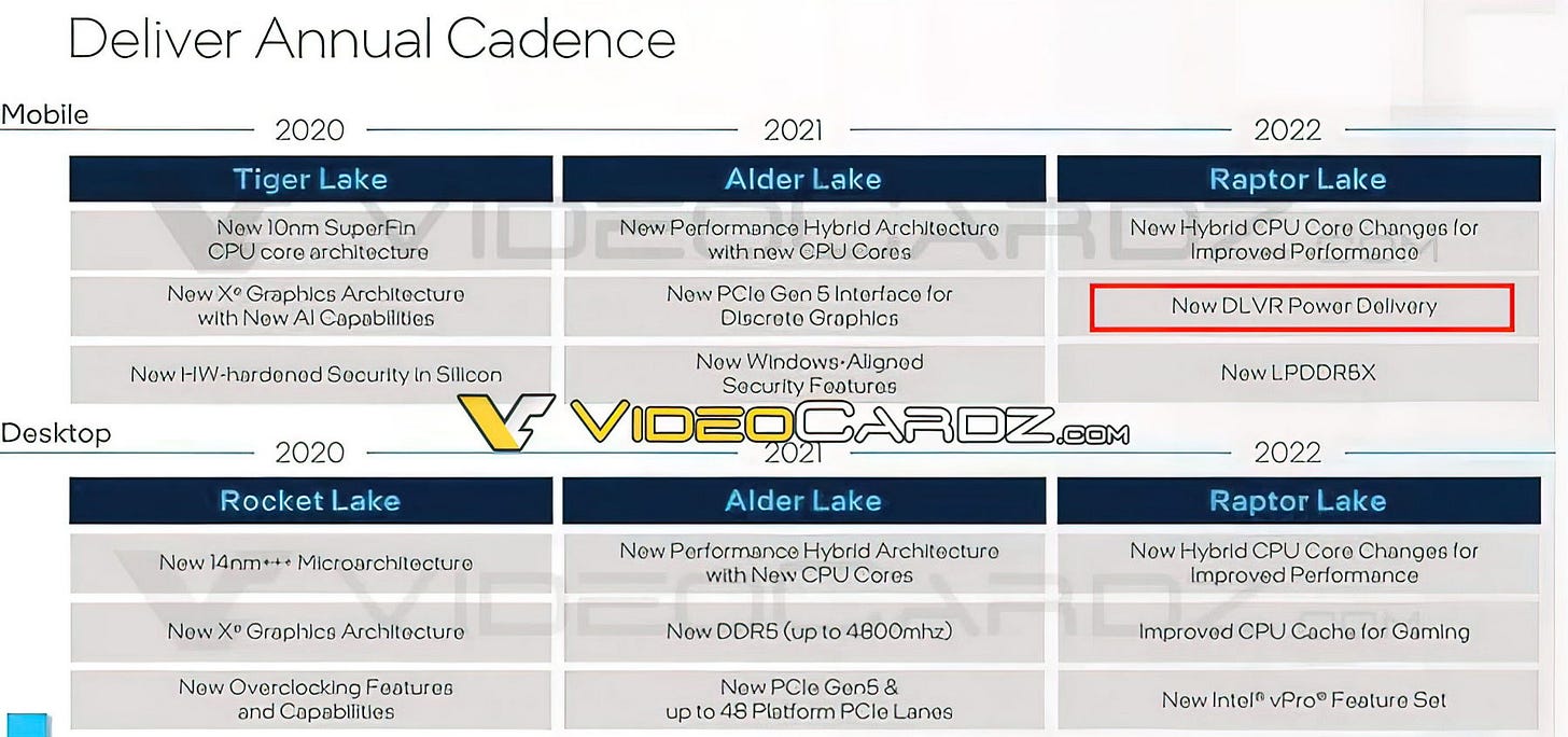
Inside the chips, Intel will likely use the same power delivery system, but maybe they won’t use the DLVRs for the desktop SKUs.
Lastly, the supported DDR5 memory speed is going up to 5600 (+ LP5X planned for mobile).
In terms of expected changes, I think that’s it.
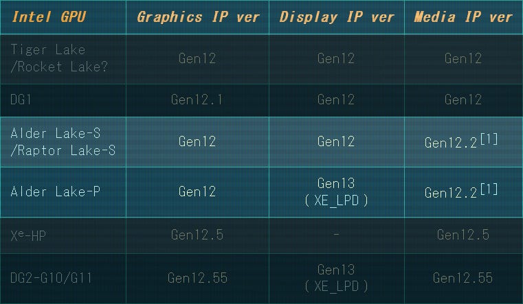
Raptor Lake-S is actually following the same IP set as Alder Lake-S, so the display version is still at v12 and not at the newer v13 found in ADL-P/M/N.
One could quickly build a mockup of the Raptor Lake-S floorplan and roughly estimate the chip size, by just adding two E-Core clusters and a bit of height for the larger L2 cache.
For that, it’s possible to take the 2 MB L2 cache design from the server variant of Golden Cove as a blueprint, but layout changes will immediately come to mind.
The server version has other storage cells next to the 768 KB L2 SRAM, which limit the horizontal playroom and led to an L2 layout which takes more vertical space.
For the client variant, Intel will most likely place more L2 cache cells horizontally, reducing the height and overall chip size requirements.
To some degree one doesn’t even have to guess, as there might be no other option, since Expreview already delidded a Raptor Lake sample, revealing the die size of it:

It’s 23.8 mm x 10.8 mm = 257.04 mm², 23% larger than the Alder Lake-S die with 20.4 mm x 10.2 mm = 208.8 mm².
The little increase in height is not enough to cover the vertical layout of the Golden Cove Server L2 cache design.
Note that in the image above, no scribe line margin is considered.
It's hard to tell if Intel could increase the density of the LLC and ring design to make some vertical room.
Rather, let's assume that Intel will make the L2 cache layout wider.
That way we can fit everything inside the box and keep a border:
A look at the simple mockup does present a lot of unutilized silicon space around the uncore and GPU area now.
Will it look like this in the end?
To some extent I wouldn't be surprised to see a lot of unused area, since Comet Lake and Rocket Lake weren't that area efficient either, but obviously there are some details to wonder about.
Perhaps there is some padding between the E-Core clusters, reducing the currently large borders, though they would be still surprisingly large.
The L2 cache design of the E-Clusters is also an interesting aspect to look forward to, Intel could switch the SRAM macros and not just stack the same cells on top like I did for the mockup.
By default, I assume that vendors try to reuse as much as possible, especially for projects which have a tight time schedule like Raptor Lake-S.
But it's not out of question that Intel might have done some interesting layout changes.
That's it for this info snack, see you later space cowboys (girls):
______________
Subscribe for free to receive a newsletter when new content is available.
If you would like to support this work financially, you can choose the paid newsletter option or go to my Patreon page and select a tier that suits your budget - https://www.patreon.com/locuza

