Die walkthrough: Alder Lake-S/P and a touch of Zen 3

I try to make at least one video project per month and in January I was bouncing back and forth between three different projects.
All of them need or needed many more hours in addition, to get to the finish line, so instead this short (back then) rambling piece was started instead.
Well, it obviously did not make it for January, February, March, April or even May.
But now it’s here!
We will look at two different Alder Lake chips, one for the desktop market and one for the mobile segment, but we won't cover everything in great detail.
I already wrote about Tiger Lake with 4 and 8 cores, Rocket Lake and Alder Lake on Patreon, so if you want more details and to know about some structure sizes, you can look it up there:
https://www.patreon.com/posts/57887608
It’s probably the third time I’m doing Alder Lake-S annotations.
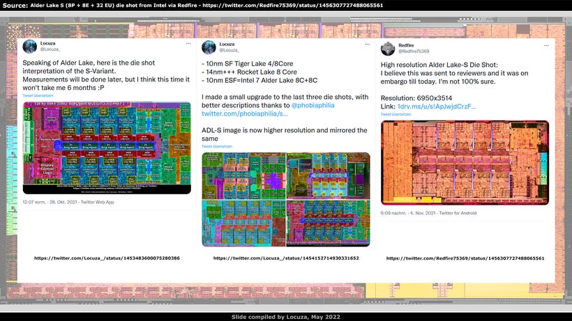
The first one was based on blurry wafer shots, later on a better resolution image from Intel’s newsroom, I also changed the orientation once and then Redfire uploaded a high-res image from Intel’s marketing department and I was obviously, ohh boooi, here we go again…, but quite quickly Nemez presented their great die shot interpretation based on it, so the job was already done and I felt no need to do it myself anymore:

This changed later because Intel released a high-resolution die shot of Alder Lake-P.
I would like to thank Petros, Bionic-Squash and Alex H. for the notifications!
When I’m busy with content, which is almost always, I don’t see much of the outside world.
I mean outside world of the virtual world, if that makes sense.
Anyway, let’s begin with Alder Lake-S.
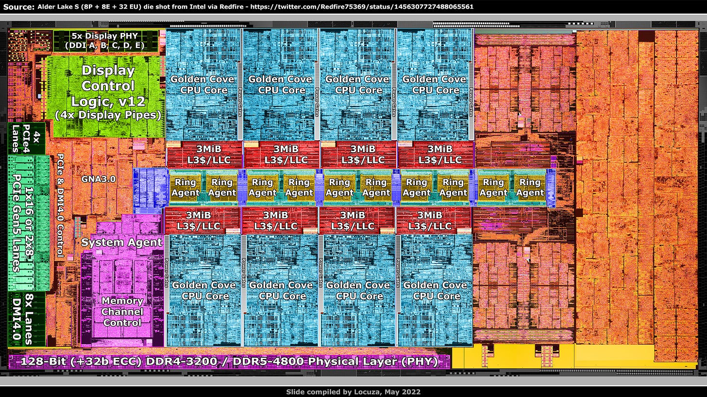
At the top left we have 5 display ports.
Below it is the display control logic version 12, with 4 display pipes, so the output is limited to 4 displays.
On the left side in the middle are the major I/O lanes to the outside world.
4x PCIe 4 Lanes, usually for an SSD and below are the PCIe 5 lanes.
The lane splitting, according to Intel’s documentation, is not as flexible as before.
Intel can provide 16x lanes to a single device or make a split with 2x8 lanes.
It’s no longer possible to have a 1x8 and 2x4 splitting.


Though, as Ryan Shrout from Intel presented, it’s possible to use a 4 lane PCIe 5 adapter on the mainboard slot to run one or two SSDs independently.
Underneath the PCIe 5 lanes are 8x lanes for the Direct Media Interface 4.0, which connects to the Platform Controller Hub ("Chipset").
Intel uses the same PHY design for PCIe 4 and DMI, so it’s possible to make a direct area comparison between PCIe 5 and 4.
It’s always fascinating to see what has changed with a new standard.
On AMD’s chips, the PHY blocks always look different and it’s not easy to tell if there is an area overhead associated with newer PCIe versions and twice the PHY speed.
For example, the PCIe 4 block on the Zen 2 and 3 client I/O die is even smaller than the PCIe 3 block on Zen 1, even though the node is basically the same.
In absolute terms, memory interface PHYs did not really get smaller or larger over the last couple of years, even when a new standard doubled the transfer speed.
In some cases one could wonder if the PHY design was previously not well optimized, overengineered or if it was in some kind of technical realm, where scaling was relatively easy to achieve.
Another big factor is the packaging design and the possible density of the I/O connections.
On Alder Lake, the PCIe 5 block is visibly not the same size as the PCIe4 block, but 36% larger with 2.4 mm² vs. 1.7 mm².
To the right should be the digital control logic for PCIe and DMI.
In addition, somewhere the Gaussian & Neural Accelerator 3.0 should be located, a low power coprocessor for AI applications like audio noise cancellation.
Then there should be the System Agent, which controls and interacts with many aspects of the SoC, like the power control unit, display, PCIe, DMI, memory and coherency management.
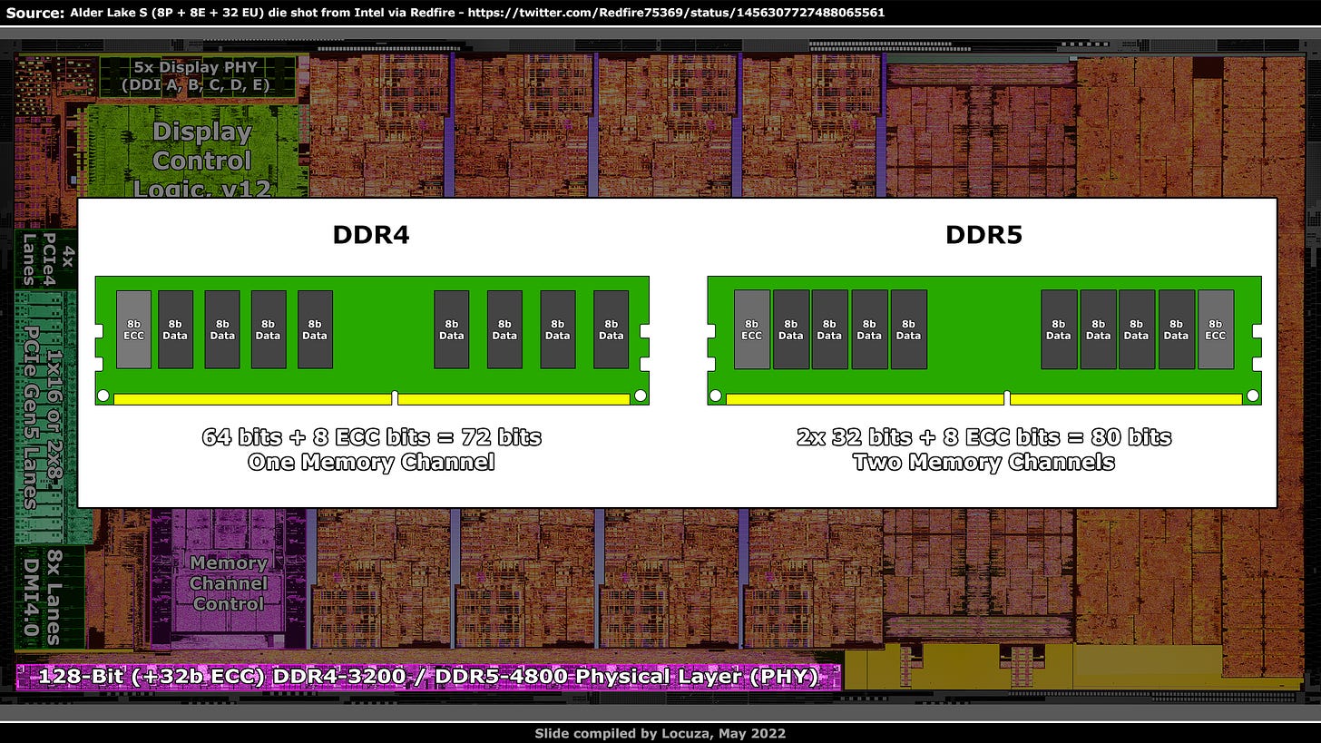
Below that is the control logic for the memory channels and at the very bottom we have the Physical Layer, which is the interface to the memory chips.
Alder Lake supports multiple memory standards including DDR4, DDR5, LPDDR4(X) and LPDDR5.
That brings in some extra complexities, since each memory standard has different specifications, like memory channel width, timings, voltage levels, and so on.
For Alder Lake-S only support for DDR4 and DDR5 is granted, although the chip likely could also support LPDDR.
Alder Lake-S does support ECC, Error Correction Code, so the memory interface should actually be 160 bits wide.
Each DDR5 DIMM has two (sub) memory channels, while DDR4 DIMMs only provide one and 8 bits per memory channel are used for ECC.
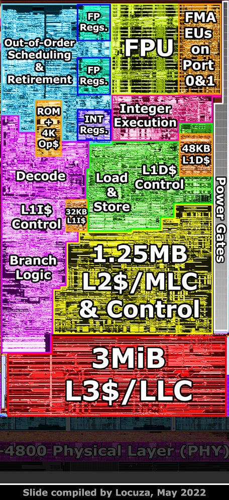
Moving to the middle, where we see 8 performance cores, called Golden Cove.
They are relatively large and it’s an interesting discussion field how this will evolve in the future.
Every company has to pick a sensible compromise between performance, power and area.
Golden Cove won the performance crown per thread by quite a bit and the efficiency, at least for higher frequency & voltage points, looks good.
It’s area, where one may wonder if Intel will focus a bit more on compute density per mm², as AMD will provide 96 cores with Genoa, followed relatively quickly by Bergamo with 128 cores and the ARM competition will also provide over 100 cores.
Sapphire and Emerald Rapids are in the 60 core realm, and while Intel could win on a per thread base or when using specialized hardware like AMX, they won’t be competitive in many general compute applications.
In that regard, I’m curious to see what approach Intel will pick going forward.
Anyway, for now Golden Cove is Intel’s horse in the race and let’s check it out a bit.
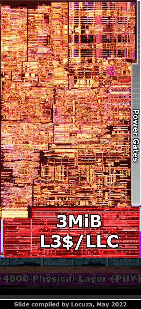
The die shot is not showing the transistor level, but a few metal layers above it.
As such, we don’t see the SRAM cells and digital logic, what we do see however are black lines or seams, which should separate multiple subunits of the CPU core.
Since Intel is using basically the same high-level floorplan since over a decade, it’s relatively easy to tell what is behind those sub-blocks (on a coarse level).
In the top left is the out-of-order and retirement logic, in the middle are the register files for floating-point and integer execution units, which are found on the right side.
In the bottom left, in purple, should be the frontend design, which includes the branch prediction machinery, decoding, a microcode ROM, an Op-Cache and a 32 KB small Level 1 Instruction Cache.
The green block to the right is handling load & store operations and has the 48 KB sized Level 1 Data Cache.
In yellow, at the bottom, is the private Level 2/Mid-Level-Cache subunit, with a capacity of 1.25 MB.
There are a few details which you obviously can’t see on this die shot, like the position of the L1 Caches, the microcode ROM and the Op-Cache.

Fortunately Yuuki Ans and Bigic uploaded die shots of Sapphire Rapids, which uses basically the same core with some extra hardware for different submarkets.
Like another set of AVX512 execution units on Port 5, AMX for machine learning applications, an extended L2 cache, a smaller L3 cache capacity and the scaling is done via mesh interconnection, instead of a ring bus.
Thanks to Chester alias Clamchowder, who brought up a line of arguments how the Op-Cache and microcode ROM looks like on Sandy Bridge, it was very easy to find the same basic structures on Golden Cove.
So credits for that point goes to him:
Clamchowder on Twitter - https://twitter.com/lamchester
There is also an important caveat I have to mention at this point.
While the core breakdown physically appears to look that way on a metal layer, logically the annotations are simplified and do not 100% correctly reflect what is inside a subunit.
For example, the store buffers are found inside the integer execution block and not in the load & store area.
Better die shots could help here, but at this level it's in general hard to precisely tell which elements logically belong to a subunit.
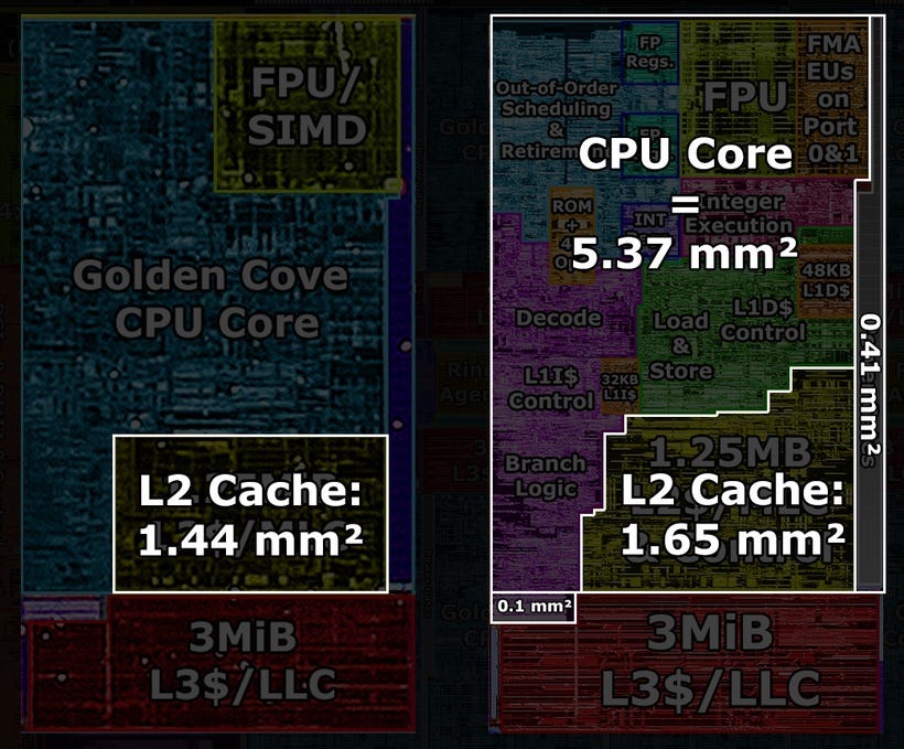
Back to the Level 2 cache.
The yellow area is larger than the coarse rectangle box I drew previously on annotations.
This shows an obvious issue in relation to fair CPU core comparisons, it can be hard to impossible to do so.
Some simplistic selections may include more or less logic than what actually belongs to the core or specific subunit.
For example voltage regulation, clock generation, multiple larger sensors and a bus/fabric unit could be included, which are not taken into account for the other comparison point.
There are cases where it’s not possible to precisely filter everything out.
And even if it is possible, you have to be careful with the conclusion.
Products don’t just use CPU cores in isolation, but a complex system architecture.
Company A may have a great expertise in CPU core design and invest into large cores, while company B may choose smaller cores, but spend more area on the cache system, the fabric and memory controlling.
At the end of the day, you might get similar performance and area results for the whole SoC, but if you would just compare the CPU cores, one could think the cores from company A have a terrible performance per mm², which is not correct and way too simplified.
So we have to keep that in mind when we look at CPU core comparisons.
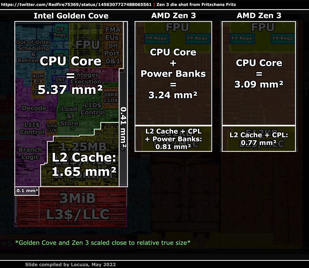
That said, I estimate a Golden Cove core with the L2 Cache and Power Gate stripe to be around 7.43 mm².
Without the Power Gates, the core size goes down to about 7.02 mm².
There is a small core piece that extends into the L3 Cache area, it may include clock driver circuitry, which is why I excluded it, but if you want to add it, it’s 0.1 mm² small.
The L2 Cache area appears to take roughly 1.65 mm², while previously I only subtracted 1.44 mm².
So the CPU core alone measures more like 5.37 mm².
Zen 3 from AMD, with small power banks on the right and left side, only needs 3.24 mm².
The L2$ tile with some test logic about 0.81 mm².
Without the power banks, the core occupies just 3.09 mm² and the L2 Cache tile shrinks to 0.77 mm².
So approximately the CPU core area, without private Level 2 Caches, is 74% larger on Golden Cove compared to AMD’s Zen 3.
In addition, we can look at other comparisons.
One is to make a selection for the whole 8-core complex, with the respective L3 Cache slices.
On Alder Lake that area is about 84 mm².
For AMD’s desktop Zen 3 CCD, we are looking at roughly 68 mm².
From this perspective, the Alder Lake configuration takes up only 24% more space.
If you would exclude many important aspects and just look at the total cache capacity, that would be even a fair comparison.
There are 10 MB of L2 Cache on Alder Lake, plus 24 MB coming from the L3 Cache, while on Zen 3 the L2 Cache accounts for 4 MB and the L3 Cache for 32 MB.
So in total it’s 34 vs. 36 MB, completely ignoring different SRAM designs and so on.
It’s not possible to test this configuration on Alder Lake, but you can disable the efficiency cores and still have access to all 30 MB of L3 Cache.
That would roughly add 6 mm² and it would be 40 MB of Cache on Alder Lake vs. 36 on Zen 3.
In total, the Alder Lake setup is then 33% larger and the performance per mm² doesn’t appear that far off anymore.
3DCenter compiled the average performance advantage of the 12900K in games, based on many launch reviews, which was about 15% in front of the 8-Core 5800X Zen 3 CPU.
With only the P-Cores enabled, the gaming performance is a bit better on Alder Lake, with DDR4 about the same or a bit worse, so 15% should also more or less apply to our comparison.
In addition, the energy consumption is not so different in games, but it really depends on the application and both SKUs are not using the sweet spot on the voltage-frequency curve.
For this analysis we only care about the performance per mm², which is of course also tight to the power budget, but it’s really hard to get a detailed and fair comparison here.
So we are just glad that the energy consumption appears to be relatively close together.
In AMD’s favor, we could hypothetically remove the large stripes for the TSV interconnection with a 3D Cache, since untill recently that was a useless area overhead for consumer products.
It would net us about 3 mm² and make the Alder Lake setup 39% larger (64.78 vs. 90.08).
On the other hand, we could also remove a bit of area for Golden Cove, since Intel really doesn’t want the AVX512 capabilities to be exposed, which increase the size of the register files and execution units.
Without considering core floorplan challenges, you may in theory gain about 1 to 2 mm².
Depending on how generous one is for a particular vendor, the performance per mm² advantage of AMD’s 5800X seems to be in the 15-21% range.
That’s far less than the 51% advantage if the end performance would have been solely attributed to the CPU core area without L2 and L3 caches.
Obviously, even with the 8-core complex with caches, we did exclude numerous aspects like the memory controllers and the fact that AMD uses a separate 12 nm I/O die.
But I think comparing the 8-core compute engines is as close as we can reasonably get for a somewhat fair and simple comparison.
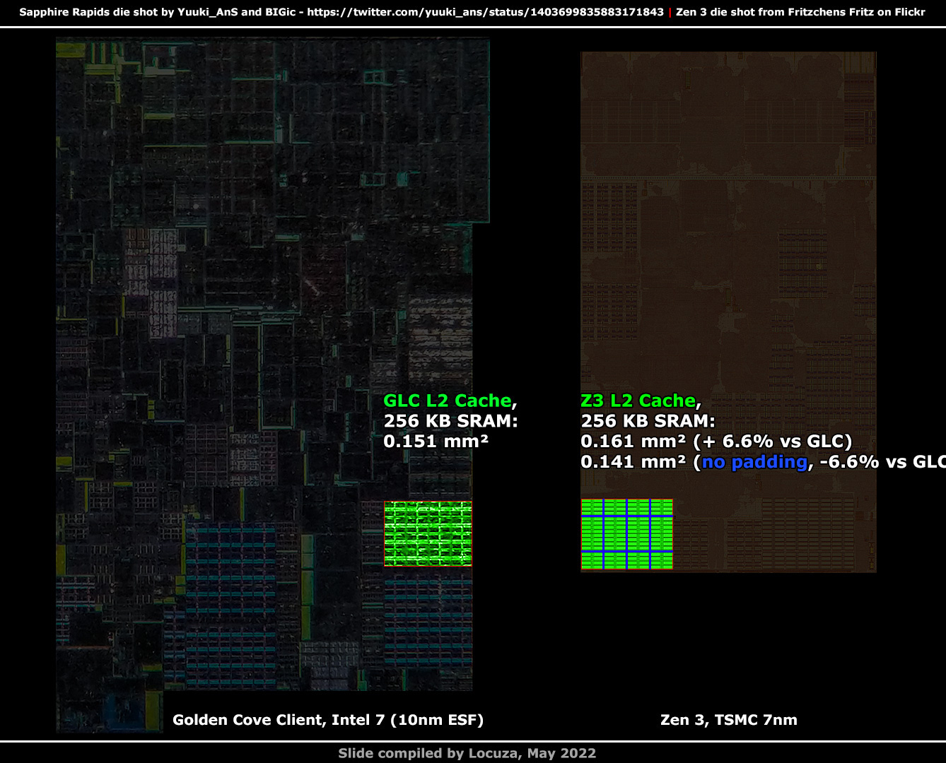
One last data point in that regard, the area consumption of 256 KB of L2 cache.
Alder Lake is made by Intel’s 10 nm Enhanced SuperFin process, which Intel later renamed to Intel 7, to align more closely to what the competition like TSMC is offering.
Based on previously disclosed specifications, it was estimated that Intel's 10 nm process offers an even better density than TSMC's 7 nm node.
Around 11%, which makes it clear why Intel renamed it later.
Though, in regard to the size of high-density SRAM cells, TSMC is smaller.
Intel’s initial 10 nm process had terrible yields, and some reports claimed that the specifications got revised for later 10 nm nodes at the expense of density.
I'm not sure if it's true and if it would have affected the SRAM density.
Let’s just look at what we see.
Well, AMD’s 256 KB L2 SRAM area takes up 7% more space than Golden Coves.
Not exactly what I would have expected based on AMD’s mixed design language between high-density and high-performance, but there are a few explanations why the selection is larger on AMD’s side.
Potentially the scribe line margin of 3% is too large on Intel’s side and I underestimate the structure size on Golden Cove a bit.
Moreover, it does look like the SRAM array on Golden Cove is very tightly packed, while on Zen 3 there is more space and logic between the Cells.
If we take the optimal case and remove the padding on Zen 3, the size would be 12% smaller than before and about 7% smaller vs. Golden Cove.
Overall close together, but as mentioned, the precision is limited by an unknown scribe line margin and the low-resolution of the Sapphire Rapids die shot.
From a more coarse perspective, the Golden Cove L2 cache subunit takes 1.646 mm², while on Zen 3 the L2 cache unit needs 0.704 mm².
The subunits may not be fully comparable, but from this perspective, Golden Cove has 7% more KB per mm² than Zen 3.
However, better density can come naturally with more or larger SRAM cells, since the control logic does not have to be scaled as much.
All in all, Intel’s L2 cache design appears good, with sensible compromises.
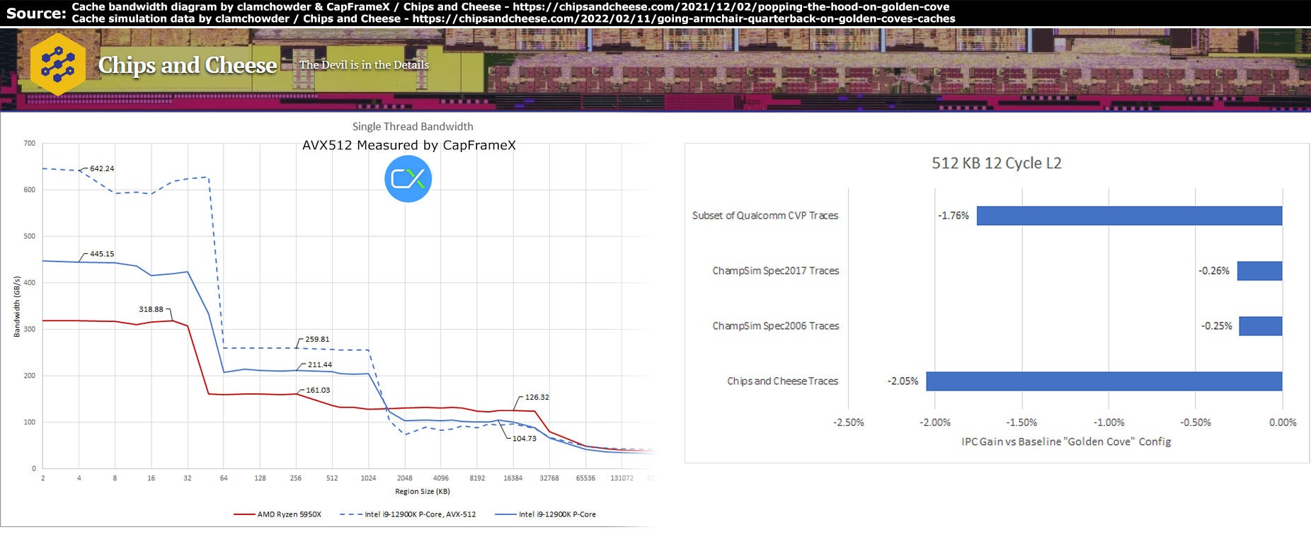
The access latency in cycles is 25% higher than on Zen 3, 15 vs. 12, which is definitely a lot, but since the clock speed is a bit better, the absolute latency is „only“ about 20% higher.
On the other hand, Intel’s cache is 2.5x larger and can provide 30-60% more bandwidth as measured by Clamchowder and CapFrameX.
Based on some simulation data from Chips and Cheese, Golden Cove could lose up to 2% IPC, if it would be using the Zen 3 L2 cache design with 512 KB.
So the larger L2 cache capacity, for this core and L3 cache system, is outweighing the negative impact from the higher access latency.
But is it worth in terms of performance per mm² ?
A simplistic calculation would say no.
A 2% reduction of the IPC, coupled with about 5.3 mm² less, would yield 4% better performance per mm².
One could go through many hypothetical models and be more precise with the selections, but let's move on to the smaller efficiency cores.
They are grouped together as a quad-core module, sharing 2 MB of L2 cache, and Alder Lake has two of such groups.
A quad-core complex requires about 8.66 mm², that's roughly 15% more than one Golden Cove with all bells and whistles.
So they don't quite occupy the same area as Intel claimed, but it's relatively close.
It's probably a bit late to say it, but all measurements are not super accurate.
Besides the scribe line margin of 3% I picked, Intel's die shot is not really well-made and shows quite ugly warpage.
I deskewed it a bit, to achieve more straightness, but it’s still not good for robust measurements.
Depending on how you do it and with or without power banks, you may land between 1.6 to 1.7 mm² for one efficiency core.
Based on the smallest numbers they just take 30% of the area of a Golden Cove core without its L2 cache and clock circuitry, respectively Golden Cove is 3.4x times larger.
That’s the cost of wide vector units, very deep buffers and a high-frequency design.
The Golden Cove FPU alone, without the vector register file, is close to about 1 mm² or 62% of one efficiency core.
Add the vector registers and you get about 77% of the area.
With the x87, MMX and mask registers on top, probably 80%.
Like holy transistor, that block unit is expensive on Golden Cove.
But the Zen 3 FPU is not cheap either, at around 0.82 mm² it takes up 52% of the Gracemont area.
However, in this case everything should be included, the Execution Units, Vector Registers and the Floating-Point-Scheduler.
If you would include all FPU related logic on Intel, you would be above 80%, potentially even approaching 90%.
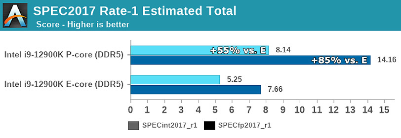
With only one thread on Alder Lake, Golden Cove is approximately 55% faster for integer workloads and 85% for floating point code in SPEC2017.
Hence it’s obvious why the small cores were introduced, one part of it was to scale up the multithreading performance for general use cases, as the area cost for that is relatively small.
Finally, a look at the media and iGPU complex.
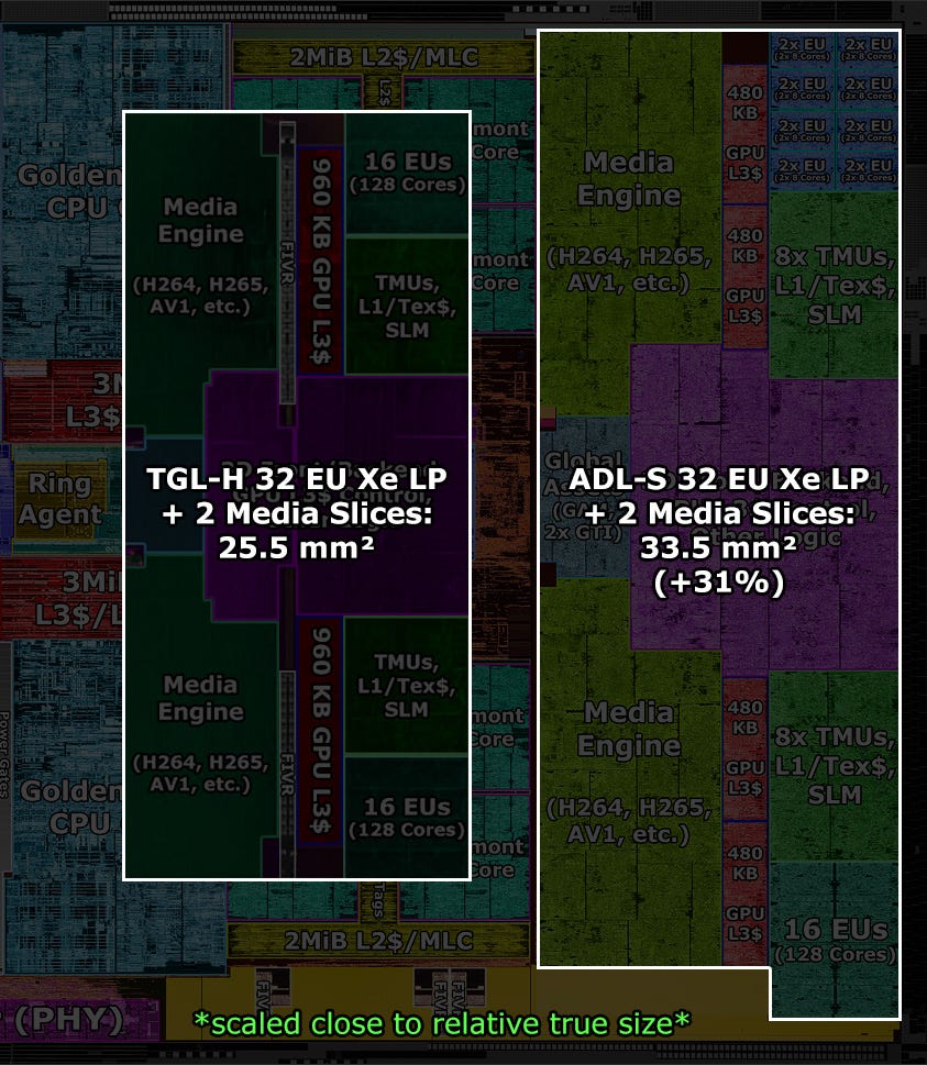
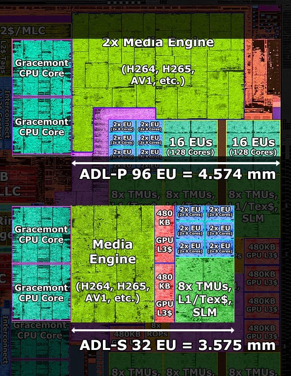
It has the same configuration as the Tiger Lake-H complex, with two media engines and a small GPU block with 32 execution units, respectively 256 shader cores.
But seeing the size difference, there is one striking question which immediately comes to my mind, like...
"Holy cow intel what are you feeding this chicken with!? It's larger than all the other ones!"
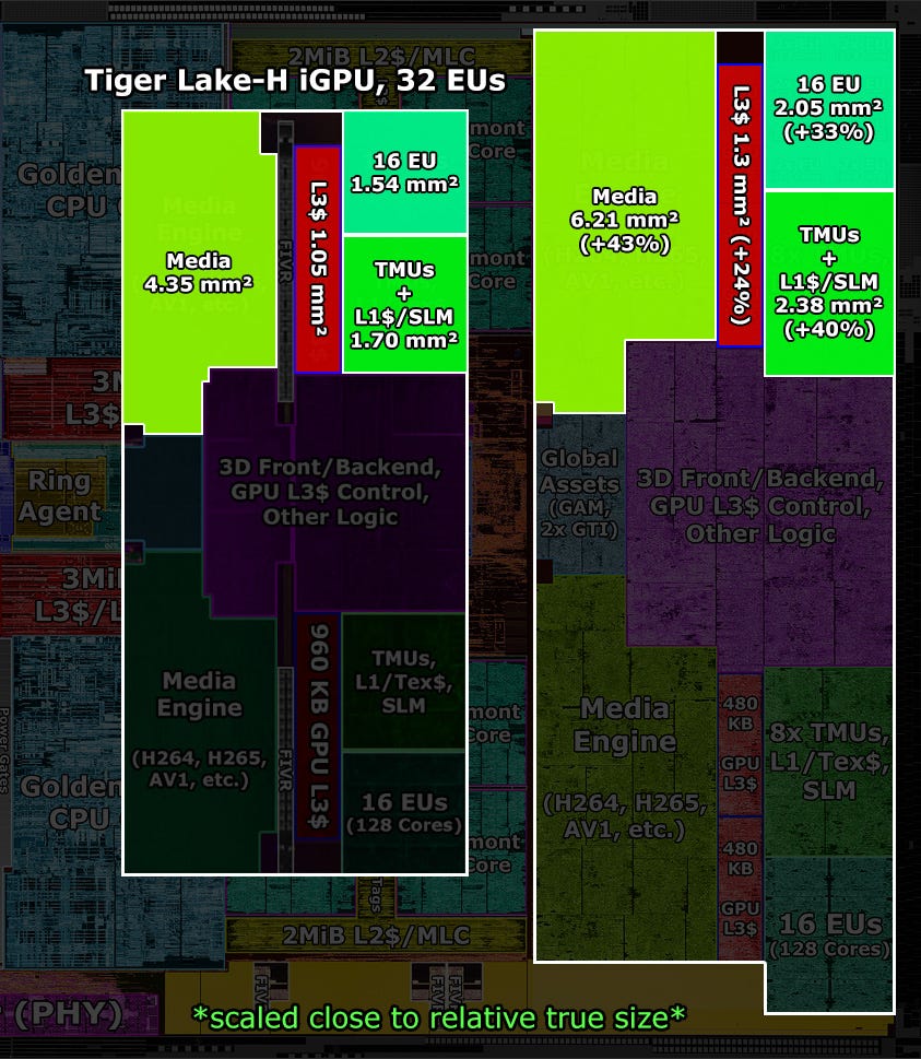
While the complex on Tiger Lake-H is only about 25.5 mm², it’s 31% larger on Alder Lake-S with 33.5 mm².
Even more if you exclude the empty space and integrated voltage regulators on Tiger Lake.
This naturally leads to the question of why is it so much larger?
The GPU IP could have the version number 12.2 or it’s still at 12.1.
Either way, no major capabilities were added like new features for DX12, Vulkan or ray tracing and matrix units.
It’s basically the same GPU as before and the product clock speeds are only slightly higher.
Instead of 1.45 GHz on Tiger Lake-H SKUs, you get 1.5 or 1.55 GHz on the top Alder Lake-S models.
Nothing that would justify this increase in area.

Fortunately, SkatterBencher tested how far you can push the frequency up.
Without even increasing the voltage, about 2.1 GHz can be set, which is 35% above the default settings!
Since the voltage is not increased, the power consumption scales in a linear fashion and GPU temps only increase slightly.
With BCLK overclocking and a much higher voltage level, 2.4 GHz can be achieved.
Unfortunately, I have not found any overclocking results for Tiger Lake devices, where allegedly there are overclockable H-SKUs.
So it’s hard to say if FMAX is much higher than before and one reason why Alder Lake-S has a larger GPU design.
In numbers, the execution units are about 33% larger than before and the texture sampler and L1 cache complex even 40%.
But not only the GPU parts are bigger, the same is true for the media engines, which also grew by 43%.
So apparently the entire GPU and media complex was reimplemented with larger design cells.
__________________________
That covers the desktop Alder Lake-S die and we can now switch to the mobile Alder Lake-P chip.
There were a couple of surprises for me personally.
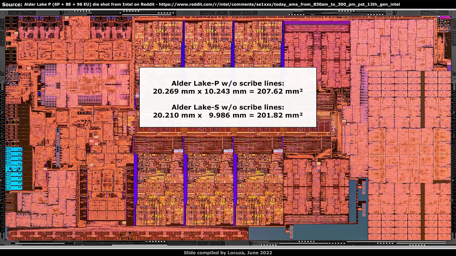
One aspect is that the P chip is only ~3% larger than Alder Lake-S.
It has two P-Cores less, but a lot of other extra features and a much wider GPU engine, which is why I had other expectations.
And we will see how Intel achieved that and what the differences are.
Starting at the top-left again, that's where Intel invested into 4x Thunderbolt 4 ports.
The bidirectional bandwidth per port can be 5 GB/s and it’s 20 GB/s in total.
That’s a lot of throughput which can be used to exchange data and to drive high-resolution display output.
The area required for this featureis quite large, around 10.23 mm².
Below is a new display engine which visually looks very different and now has the version number 13.
It still comes with 4 display pipes.
In the middle-left we have the PCIe complex.
Two PCIe 4 blocks which are intended for SSDs, each with 4 lanes.
In addition, there is one PCIe 5 block with 8 lanes.
This could be a bit surprising, because Alder Lake-P is officially not supporting PCIe 5.
Well, it really doesn’t, since the block is configured to only run at PCIe 4 speed at best.
I think Intel mentioned it somewhere that the reason was time-to-market of useable PCIe 5 devices, which is why Alder Lake-P is not supporting it.
Below that should be the Image Processing Unit, which according to Intel’s documentations is using the same logical IP as Tiger Lake-H, version 6 SE.
Following next is the memory subsystem, where at the very bottom the memory PHY is located.
It's a bit shorter than on Alder Lake-S, because this chip is lacking ECC support, saving 32 bits.
In addition to DDR4 and DDR5, vendors can also use LPDDR4X and LPDDR5 memory.
As mentioned, Alder Lake-P only uses 6 P-cores, saving a good chunk of area.
But as on Alder Lake-S, 8 efficiency cores are present.
On the right side is the GPU, with 96 Execution Cores instead of just 32.
However, the width, based on the edge of one E-Core to the end of the die, only increased by 28%.
From ~3.6 to ~4.6 mm
Intel achieved that by pushing some GPU logic in the middle, like the global assets, inside the E-Core Interconnect area.
But mostly by using the high-density implementation that is found in a similar or the same form in Tiger Lake.
Unfortunately, there are no overclockable SKUs for Alder Lake-P devices, so it will remain unclear whether the Alder Lake-S implementation can clock significantly higher.
Even if so, one has to wonder why Intel went with a larger GPU and media implementation on Alder Lake-S, when they use low stock clocks and could have saved a couple of mm² and possibly improve the yield.
Let’s wrap it up.
In the top-right corner is the lower bandwidth on-package interconnect used for the PCH, which is found on the same package as the processor.
Alder Lake-S uses DMI instead to connect to the PCH located on the mainboard.
Lastly, Alder Lake-P is also utilizing 6 fully integrated voltage regulators (FIVRs).
Unlike Tiger Lake, Alder Lake does not use them for the CPU cores, but still for the System Agent, the I/O PHYs for display, PCIe, DDR, other I/O and also for the L2 cache of the E-cores.
______________
That’s it for this piece.
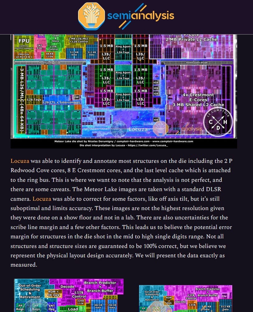
If you want to read more about the area breakdown of a Golden Cove core and see a comparison with the upcoming Redwood Coves in Meteor Lake, you can find that over on SemiAnalysis, where Dylan Patel and I covered exactly that and more:
______________
Subscribe for free to receive a newsletter when new content is available.
If you wish to support this work financially, you can go over to my Patreon page and pick a tier fitting to your budget - https://www.patreon.com/locuza


