Nvidia's Ada lineup, configurations, estimated die sizes and a comparison with other chips
Starting Info: This is old content that was written a long time ago in a galaxy far, far away, which is why it never appeared on this planet until this very moment.
What was published much earlier is an article created in collaboration with SemiAnalysis by Dylan Patel, who was also the sponsor of my parts:
The article above goes into various details, like performance and power estimates, uses a more sophisticated scaling model and more.
So, check it out in addition!
My main interest is how close we got to estimating actual die sizes, as Nvidia will likely unveil at least one Ada Geforce SKU along with the die size in the "GeForce Beyond: A Special Broadcast at GTC" live stream:
Beyond that, both articles present a very detailed breakdown of Nvidia’s GA102 chip floorplan with area measurements and a comparison with the 7 nm A100 chip and AMD’s 7 nm Navi 22 die.
A few extra and new comments were added in capital letters.
That being said, enjoy!
::::::::::::::::::::::::::::::::::::::::::::::::::::::::::::::::::::::::::::::::::::::::::::::::::::::::::::::::::::::::::::::::::::::::::::::::::::::::::::::::::::::::::::::::
In late February 2022, news emerged that Nvidia was the victim of a cyber attack, which the company confirmed.
It turned out to be of massive scale, perhaps till that point of unprecedented magnitude, including a huge amount of sensitive data
Employee credentials, stolen code signing certificates (which can be used to sign malware) and source code, leaking information about DLSS, Nvidia’s mining limiter, upcoming GPUs and more.
The next generation of GPUs will be the topic of this article.
SemiAnalysis and Locuza did not download any leaked file, however others did and shared excerpts.
In some of them, high-level information about the GPU configurations of the upcoming Ada Lovelace series from Nvidia are found.
The next GPU generation will be the subject of this article.
SemiAnalysis and Locuza did not download any leaked files, however others did and shared excerpts.
In some of them, high-level information about the GPU configurations of Nvidia's upcoming Ada Lovelace series can be found.
________________
Used sources for the analysis:
AD102-107 configurations via @xinoassassin1:


Feature table for AD102 by @xinoassassin1:
L2 cache size per Frame Buffer Partition (FBP) by @xinoassassin1.
_________________
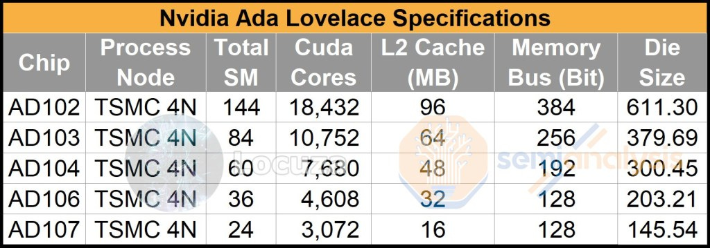
Putting the data in a table allows for a convenient comparison with the current Ampere product stack (FP32 ALU and ROP count is assumed for Ada):
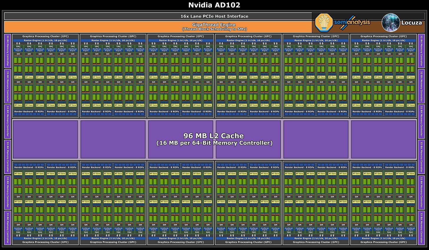
As one can see the AD102 is a huge leap forward utilizing 12 GPCs and likely 18432 FP32 units, a 71% increase compared to the GA102!
One can expect that at launch we will not see fully enabled chips and that multiple SKUs will be offered with a reduced core count.
Besides the core count, it is claimed by kopite7kimi that the L2 cache might also be reduced and that the RTX 4090 will only use 72 MB of the physically present 96 MB (disabling 1/4 of the cache banks leading to 12 MB per 64b FPB, instead of 16 MB?).
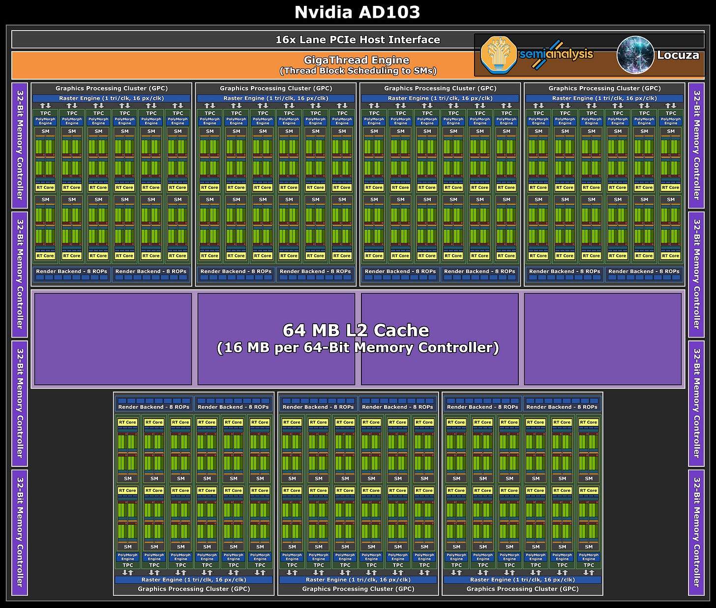
AD103 will have almost the same setup as the GA102, just with a less wide memory interface.
It’s surprising to see the large difference between AD102 and AD103 as the gap is pretty huge.
To feed the compute engines that have become wider across the stack and to compensate for the stagnant or even reduced memory interface, all Ada GPUs will include large L2 caches to keep much more data on chip.
In the case of GA102 vs. AD102, we will see a capacity uplift by a factor of 16, jumping from 6 MB to 96 MB.
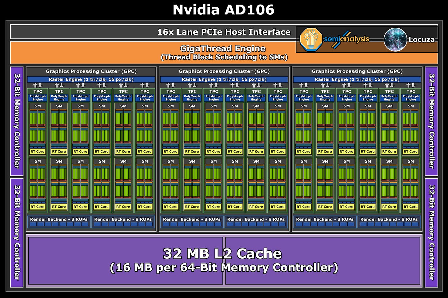
Overall there is another apparent surprise at the bottom of the stack, it’s the small difference between the AD106 and AD107 chips, which would only differ in core count, if one would assume 16 MB L2 cache per 64b FPB accross the whole Ada stack.
However, such a small difference makes little sense, which is why we believe that AD107 will physically use just half the L2 cache capacity, saving area and increasing the performance difference.
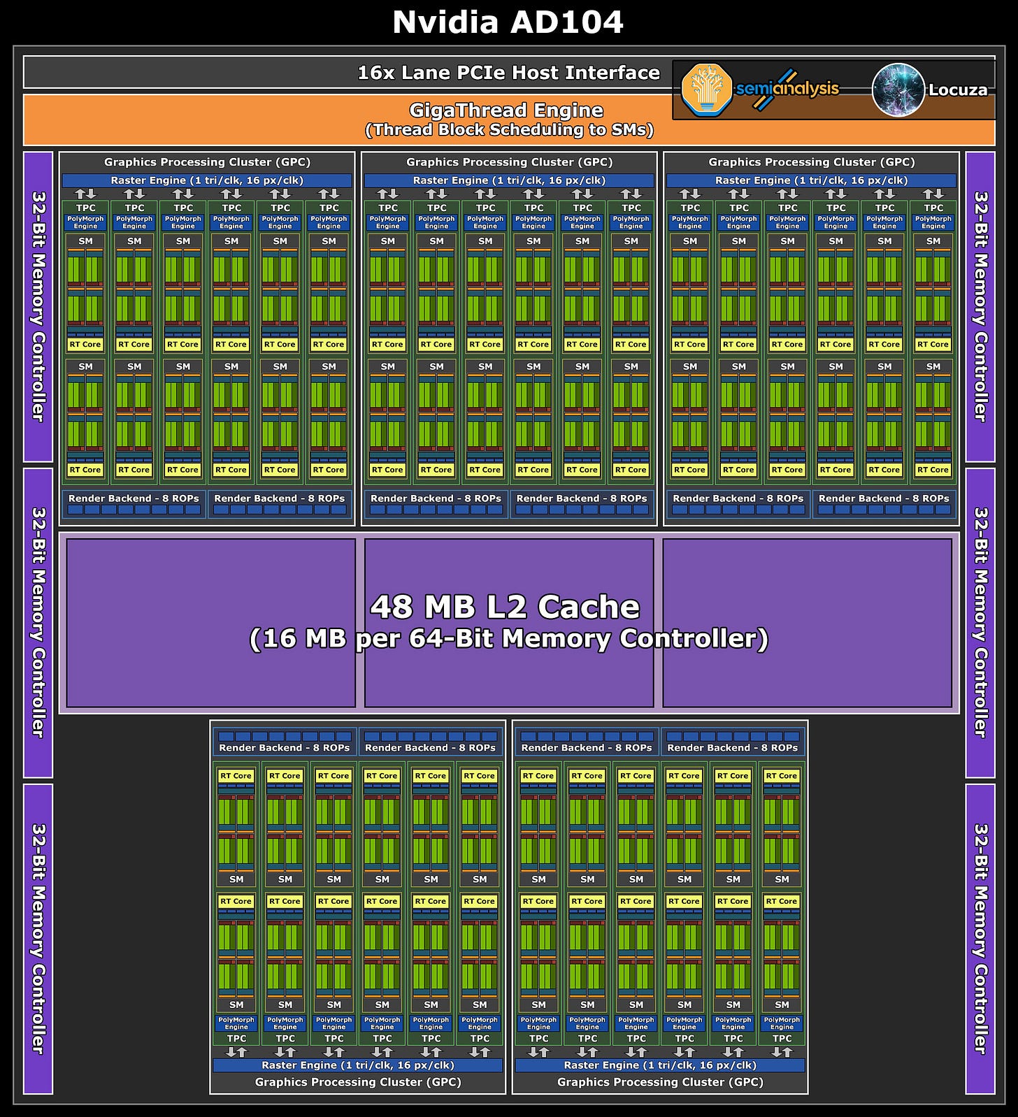
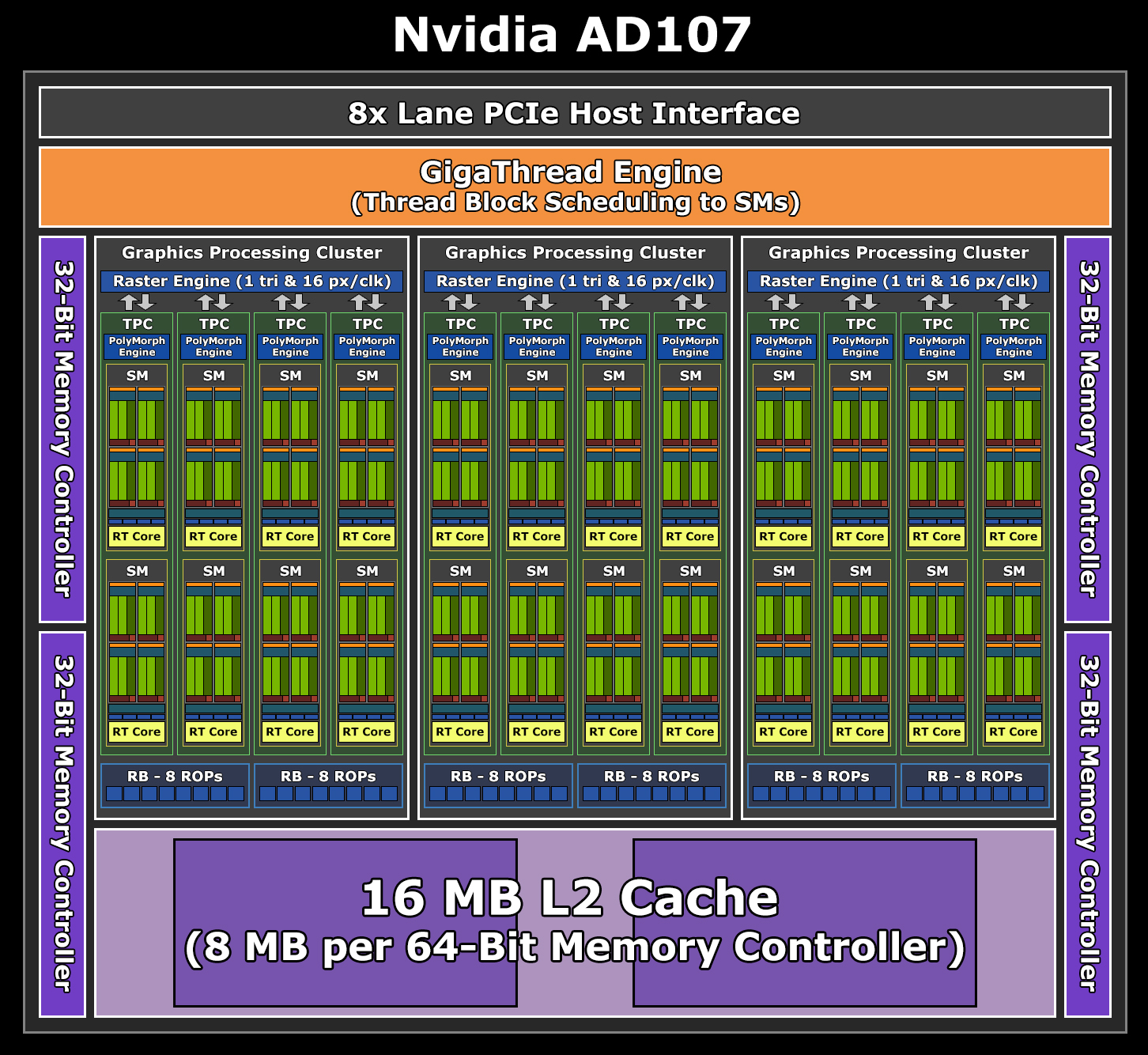
Those who prefer a visualization of the data can check out these logical block diagrams for AD102-107:
(A few updates/corrections for the diagrams could be done.
For example, it does appear that with Ada Nvidia will change a couple of scaling and organization attributes.
Similar to the Hopper H100 chip, it may be that Nvidia is introducing a new high-level unit called Compute Processing Cluster (CPC), with a fast local data share interconnection between multiple Streaming Multiprocessors (SM).
In the case of Ada, it appears that CPCs with 2 TPCs will be used.
It also changes how Nvidia is scaling parts of the fixed function geometry pipeline, as the PolyMorph-Engine (or parts of it) are not scaled per TPC anymore, but per CPC.
Moreover, AD106 may also just use 8x lanes for the now expected PCIe4 interface).
Die Size Estimates:
With the high-level configurations at hand, one intriguing question revolves around the chip sizes.
It's a tricky question that we can't solve exactly, but we'll try to approach it.
The fundamental issue is simply that the current Ampere gaming GPUs use the 8 nm process technology from Samsung, while Ada will apparently utilize a “custom” 5 nm class node from TSMC called 4N.
Between the process nodes there are different scaling factors for digital logic, SRAM and analog devices.
Moreover, there is no universal scaling factor for either device type as multiple flavors are available, and the design implementation also plays a major role.
As such, it’s impossible to know exactly where those GPUs will end up in terms of chip size.
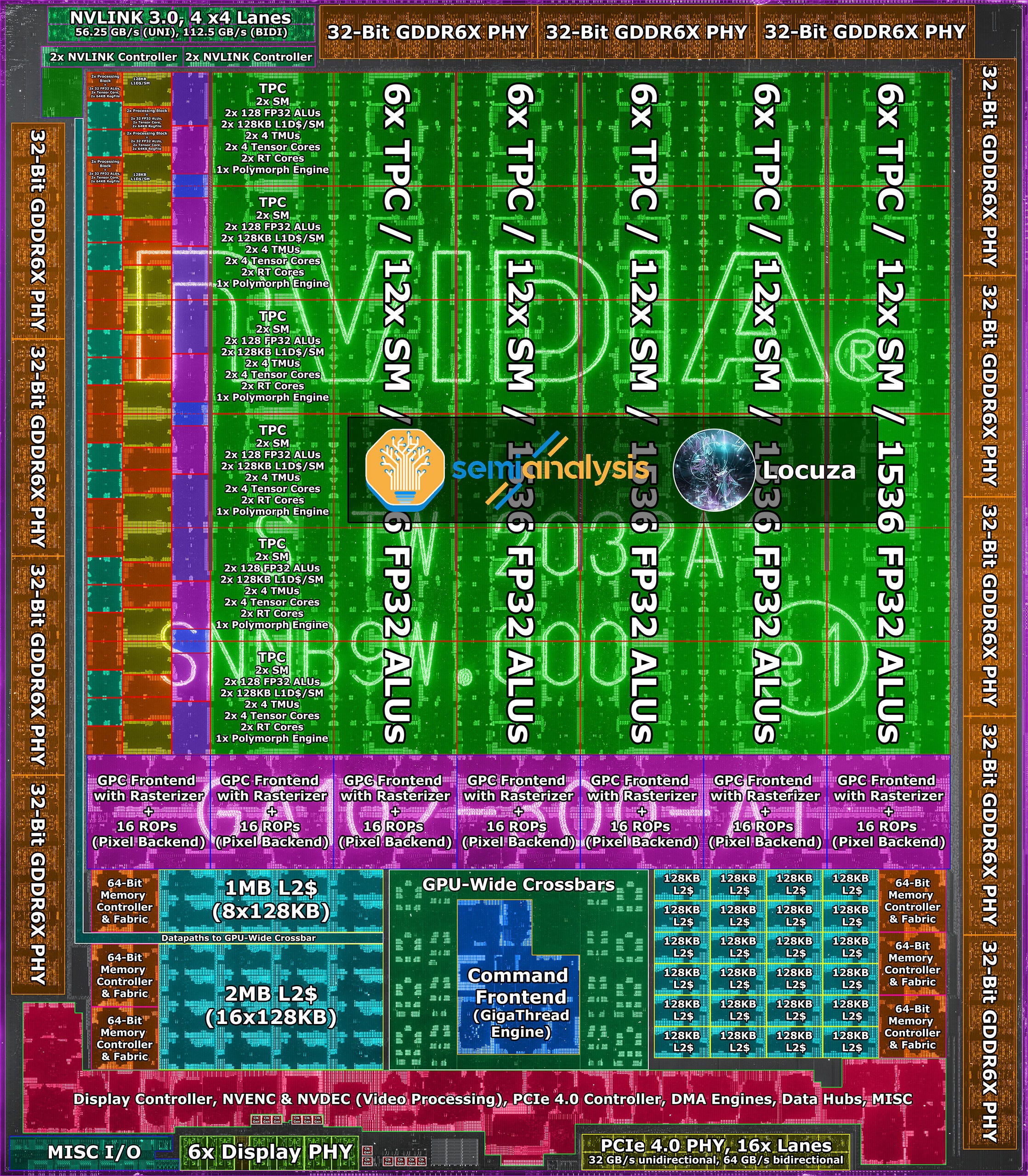
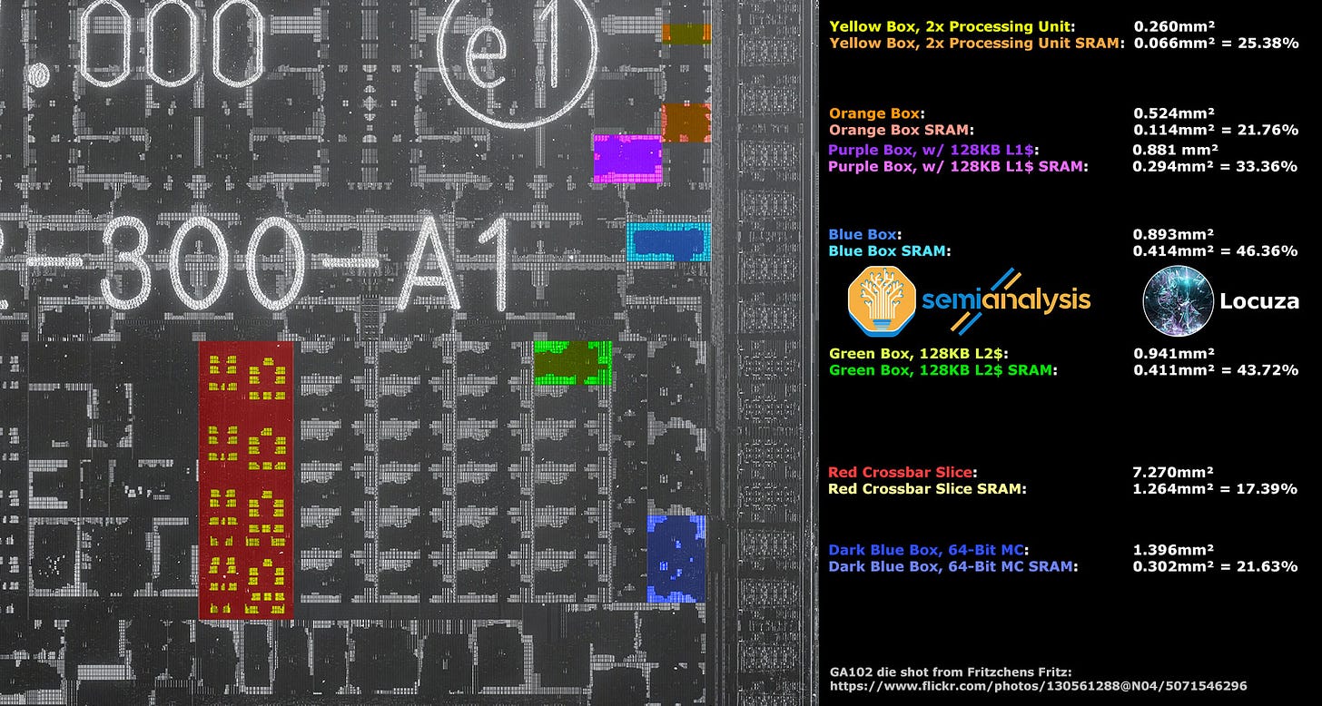
However, we can break down the area of the predecessor GA102 and use it as a reference point.
We are able to do so thanks to the excellent work of Fritzchens Fritz:
https://www.flickr.com/photos/130561288@N04/50715462966
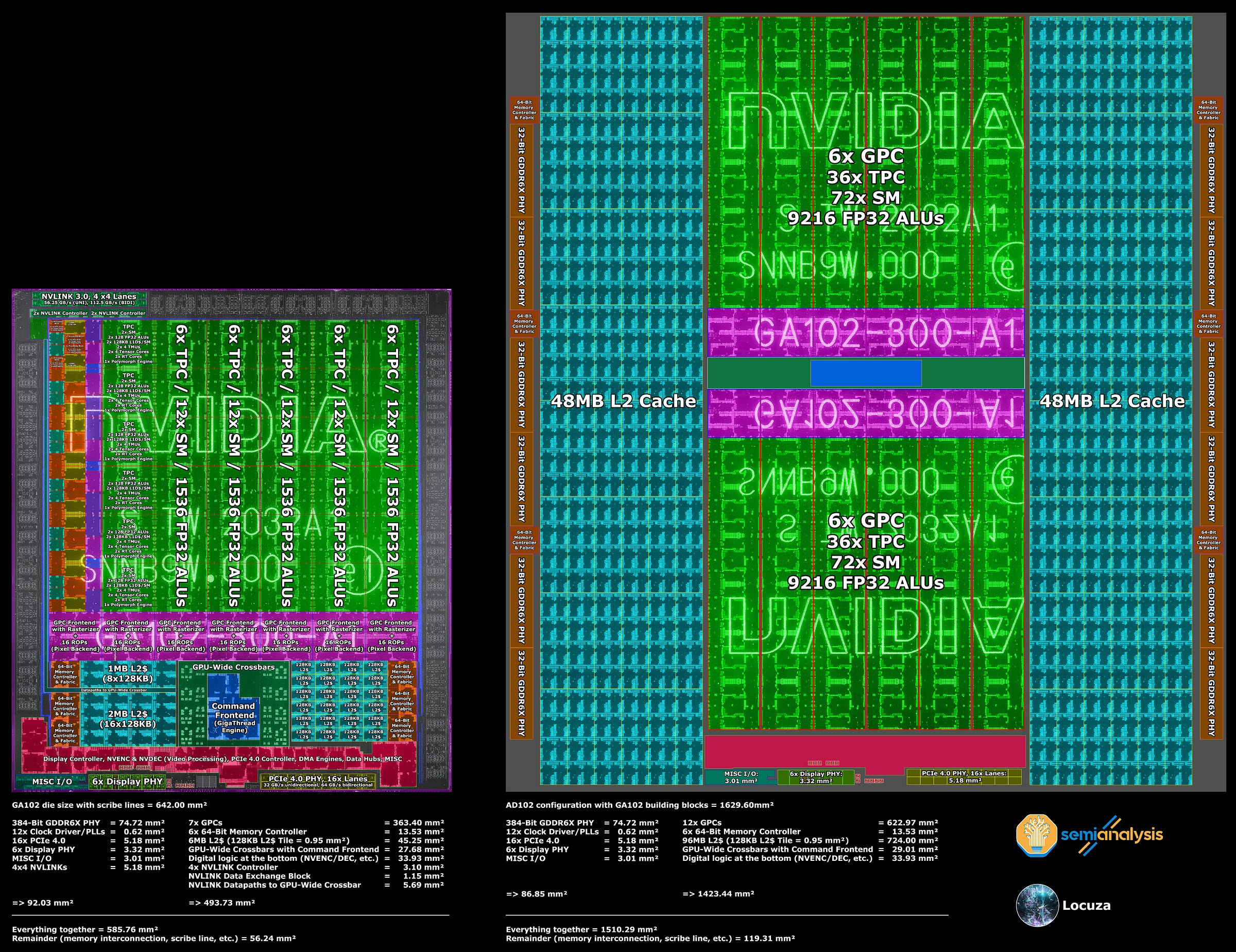
The following image shows the floor plan interpretation of the GA102 chip:
With the breakdown of digital logic, SRAM, analog devices and a small rest, one could already work on some estimates, but beforehand let’s enlarge our horizon further:
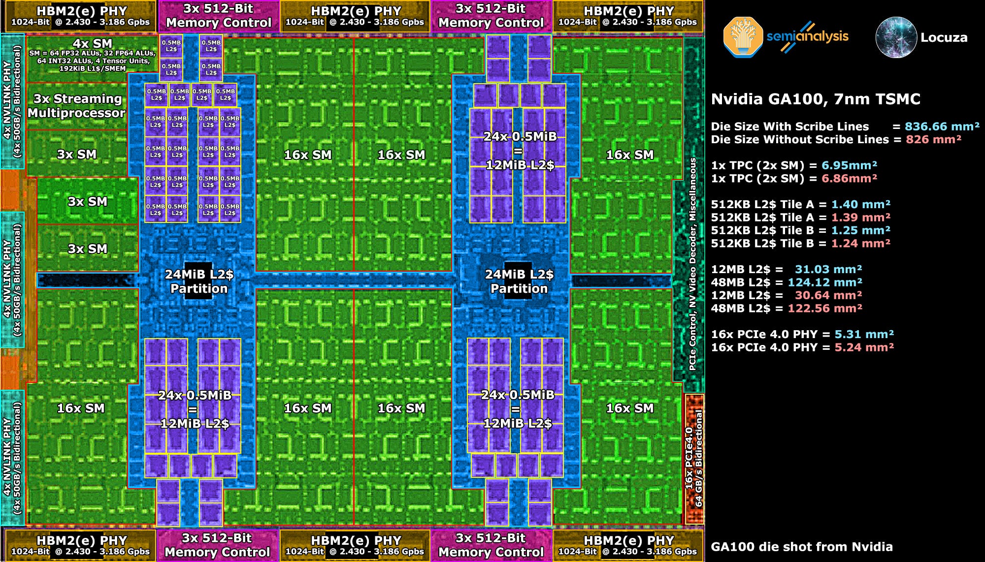
While the Gaming Ampere GPUs are made using Samsung’s 8 nm process, the GA100 chip for HPC and Machine Learning applications is manufactured by the 7 nm node from TSMC.
Unfortunately the die shot which Nvidia released comes in a low resolution which will make measurements very sketchy, but well, you can’t have your cake and eat it, life would be too easy otherwise.
Depending on whether the image contains the scribe lines or not, we get two different numbers per structure.
For the curious, one TPC requires around 6.86-6.95mm² compared to 7.46mm² on Gaming Ampere.
Though for our area estimates this doesn’t really help us as the TPC/SM design is quite different between the gaming and HPC chips.
Gaming GPUs have twice as many FP32 „units“, while the HPC variant comes with higher Tensor Core throughput and larger cache sizes, as such we are not looking at an apples-to-apples comparison.
What does provide us interesting data, is the size of the L2 cache tiles.
There are two different tile designs on the GA100 with a ~10% size difference.
The average size of the L2$ tiles would be around 1.28-1.29mm², taking ~35% more space than the L2 cache tiles on the GA102 (0.95mm²).
However, the L2 cache tiles on Gaming Ampere only have a capacity of 128 KB, while the GA100 uses 512 KB tile sizes, meaning the density is much better.
On the analog front, things turn out as expected.
16x PCIe 4.0 lanes take up about the same size as on Gaming Ampere.
Measurements of memory PHYs (DDR4, GDDR6, HBM) and PCIe3 & 4 PHYs on AMD products presented little to no scaling between the 14 nm GloFo process (licensed 14 nm Samsung process) and 7 nm TSMC.
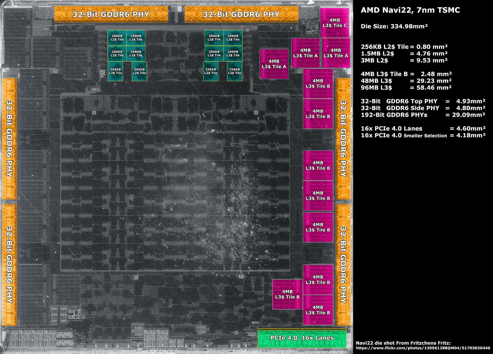
Speaking of AMD, it may be a good idea to look at the numbers of the 7 nm competition, especially since we have high-resolution die shots available, again thanks to Fritzchens Fritz:
https://www.flickr.com/photos/130561288@N04/51703830446
At roughly 0.8mm², the L2 tile size on Navi 22 is smaller than on Gaming Ampere, while providing twice the capacity.
If we simply scale up and down the area for a specific capacity, which in reality wouldn't precisely scale like that, we would get the following table:
The cache density on Navi 22 and HPC Ampere is more than twice as good, compared to Gaming Ampere.
HPC Ampere also presents a sizeable density advantage over Navi 22, if the measurement based on the blurry GA100 die shot is not significantly off.
But in terms of cache density, nothing comes even close to the L3 cache tiles on Navi 22, which AMD likes to brand as Infinity Cache.
The area requirements for 96MB can be considered to be relatively tiny, at just 58.46 mm².
But for Ada, the relative density of the new L2 cache design shouldn't be as good as AMD's L3 cache design.
It’s likely that the L2 cache on Ada will share the same clock domain as the GPU cores, achieving higher clock rates, lower latency and larger bandwidth numbers.
One last note regarding the 16x PCIe 4.0 PHY, it appears to be ~10% smaller than on Ampere GPUs.
:::::::::::::::::::::::::::::::::::::::::::::::::::
So, after gathering a small overview about structure sizes and device mixes, we could start with configurations for AD102-107, but it would still be fairly inaccurate.
While it should be relatively easy to handle the analog part, it would be largely a shot in the dark for digital logic and SRAM.
Thankfully, there are area scaling numbers which can be used as a guide from Apple’s silicon.
In addition, kopite7kimi says that AD102 is around 600 mm² large:

His track record is (was?!) very strong, and let’s give his number the benefit of the doubt, but it has to be said that this figure is obviously unconfirmed and that the following analysis stands and falls with the correctness of that number.
The easiest, and practically impossible, way to build AD102 would be to just use GA102 blocks.
It would result in this fictional monstrosity with about 1630 mm² in 8 nm:
We can keep it simple and subtract the analog portion of 86.85 mm² from 600 mm², that way we know that on AD102 the rest must be about 513.15 mm².
For the sake of simplicity we will only include the labeled blocks with digital logic and SRAM cells, while excluding the remaining area, since by and large it wouldn't matter that much.
Based on the digital & SRAM portion with 1423.44 mm², 513.15mm² are about 36% of it or from another perspective, we have to subtract the inverse with 64% to arrive at about 513 mm².
If we apply the routine for the AD102-107 configurations, we will arrive at the following numbers:
Note: The crossbar part was up/downscaled based on the amount of L2 cache tiles and necessary interconnection, for AD107 8x PCIe 4.0 lanes are assumed.
(As mentioned in the beginning, AD106 may also only include 8x PCIe 4.0 lanes.
In addition, it appears somewhat open, if NVLink will be present on the AD102 chip or not, as leaked PCB schematics do show an NVLink connector)
As can be seen, the product stack offers nice scaling, with the GPUs showing a percentage difference of 27.84 - 42.3%.
In this regard we have ruled out one configuration and that is the AD107 setup with 32 MB L2 cache.
On paper, it’s striking how small the difference would be between the AD106 and AD107 chips if both included 32 MB of L2 cache.
Of course, this is also reflected in the required area, where the percentage difference is only 9.8%.
There's no point in investing resources in developing two chips that are so close together, something definitely has to give on the AD107.
Potential cuts could be made in display PHYs and video capabilities, but ultimately the gains would be negligible to small.
However, halving the L2 cache seems like a natural solution.
It would align with the approach Nvidia took with the Turing series.
While the larger TU102-106 chips used 8 x 128 KB L2 cache tiles per 64-bit framebuffer partition, the smaller TU116 chips used half the amount, namely 4 x 128 KB L2 cache tiles:
Now, our approach above was very simple, using an unrealistic mixture of structure sizes and only one scaling factor for every block which is not an analog device.
One can try a more reasonable setup by reducing the L2 cache area that goes into the AD102 configuration while adding a separate scaling factor for the L2 cache.
The goal is to achieve a more realistic ratio of logic and SRAM cells for the AD102 mix.
The reason for this method is that each block has a different ratio:
If we go through a few structures on the GA102 chip, we see an average ratio of almost 70:30 (Logic:SRAM).
The 128 KB L2 cache tiles have a ~56:44 ratio, AMD's 256 KB L2 cache tiles on Navi 22 share nearly the same with 57:43.
Nvidia's GA100 with 512K tiles shows an inverse ratio of 43:57.
As process nodes advance, SRAM cells become more difficult to scale down, and since the L2 cache on Ada should take up a significant portion of the total die area, we probably over/underestimated the scaling of multiple chips.
If you use a more sophitasted model (and a different starting point, with a few other considerations), you get the following table:
Not too dramatically different compared to the simple model above, but hopefully still closer to the real chip sizes.
Let’s see how it turns out!
::::::::::::::::::::::::::::::::::::::::::::::::::::::::::::::::::::::::::::::::::::::::::::::::::::::::::::::::::::::::::::::::::::::::::::::::::::::::::::::::::::::::::::::::
Subscribe for free to receive a newsletter when new content is available.
If you would like to support this work financially, you can choose the paid newsletter option or go to my Patreon page and select a tier that suits your budget - https://www.patreon.com/locuza


