Nvidia's AD102 officially revealed, how close were the previous estimates?
Life after the livestream...
The previous posting covered an old estimate of Nvidia’s upcoming Ada Lovelace GPUs in regard to the configurations and die sizes:
A few hours ago, Nvidia held a keynote, revealing the first three dGPUs based on Ada Lovelace and sharing a bit more information about the top AD102 chip used by the RTX 4090.
The high-level points should be well covered by the mainstream media outlets.
So I will just add a few points that I found particularly interesting.
1.) Not shown but shared via Ryan Smith from Anandtech is the die size of AD102, it takes 608.44 mm² and integrates 76.3B transistors:
The AD102 estimate from SemiAnalysis (611.33 mm²) came very close to it, and kopite7kimi’s claim of ~ 600 mm² was right.

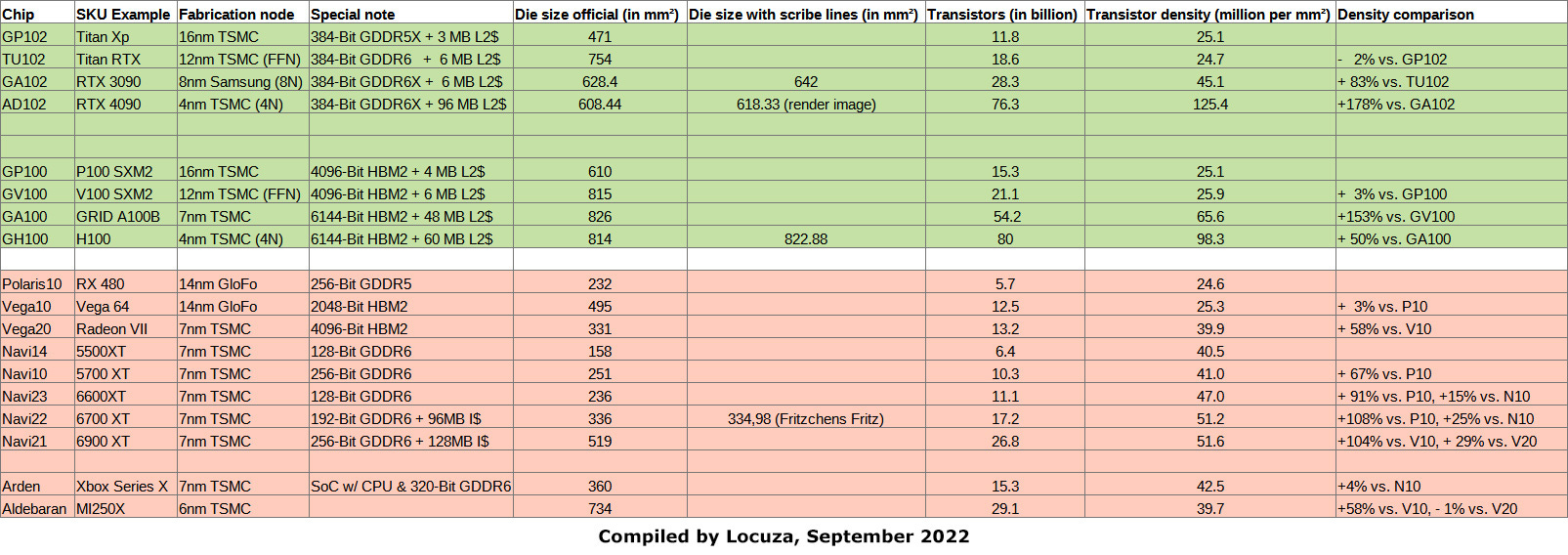
I took the opportunity to compare four generations of Gaming and HPC/AI chips.
After the 16 nm Pascal GP102 chip, Nvidia introduced the new Turing architecture, which doubled the vector register file per SIMD lane and increased the cache/shared memory capacities.
In addition, it was packed with several new features, Tensor Cores, Ray Tracing Cores, Async Compute improvements, VRS, Resource Heap Tier 2, Mesh Shader support and so on.
Everything together led to a large jump in area from ~471mm² to ~754mm².
The “12” nm node also presented itself as a simple marketing spiel, which is played since many years if not decades.
The transistor density even decreased compared to the previous GP102 chip design.
After that, Nvidia switched to Samsung’s foundry for the entire Ampere gaming line-up.
In terms of transistor density, this still resulted in a respectable 83% increase over the previous TU102 chip.
AMD achieved less going from the 14 nm GloFo nodes to 7 nm TSMC, at least for the first chips, RDNA2 with a large last level cache is showing how you can quite easily drive up the transistor count.
Now, with AD102 the transistor density skyrockets to 125.4 MTr/mm², an increase of 125.4%!
The progression on the HPC/AI side is a bit more apples to apples, as the foundry of choice was always TSMC.
Pascal GP100 offered 25.1 MTr/mm², funnily enough Gaming GP102 had the same transistor density, while Volta GV100 only provided 3% more.
Contrary to the gaming lane, the HPC/AI chip went down to the 7 nm TSMC node and offered even 153% better density vs. the previous generation!
The huge increase in L2 capacity certainly helped in achieving those numbers and
TSMC’s 7 nm node is far superior in terms of possible SRAM density than Samsung’s 8 nm process (see the previous posting), and is likely also providing significant benefits for digital logic as well.
The following Hopper step may look disappointing in comparison, only achieving 50% better density with the “custom” 4N node from TSMC.
Perhaps somewhat surprisingly, the AD102 chip, with supposedly 96 MB of L2 cache, boasts a 28% better transistor density than the Hopper GH100.
2.)
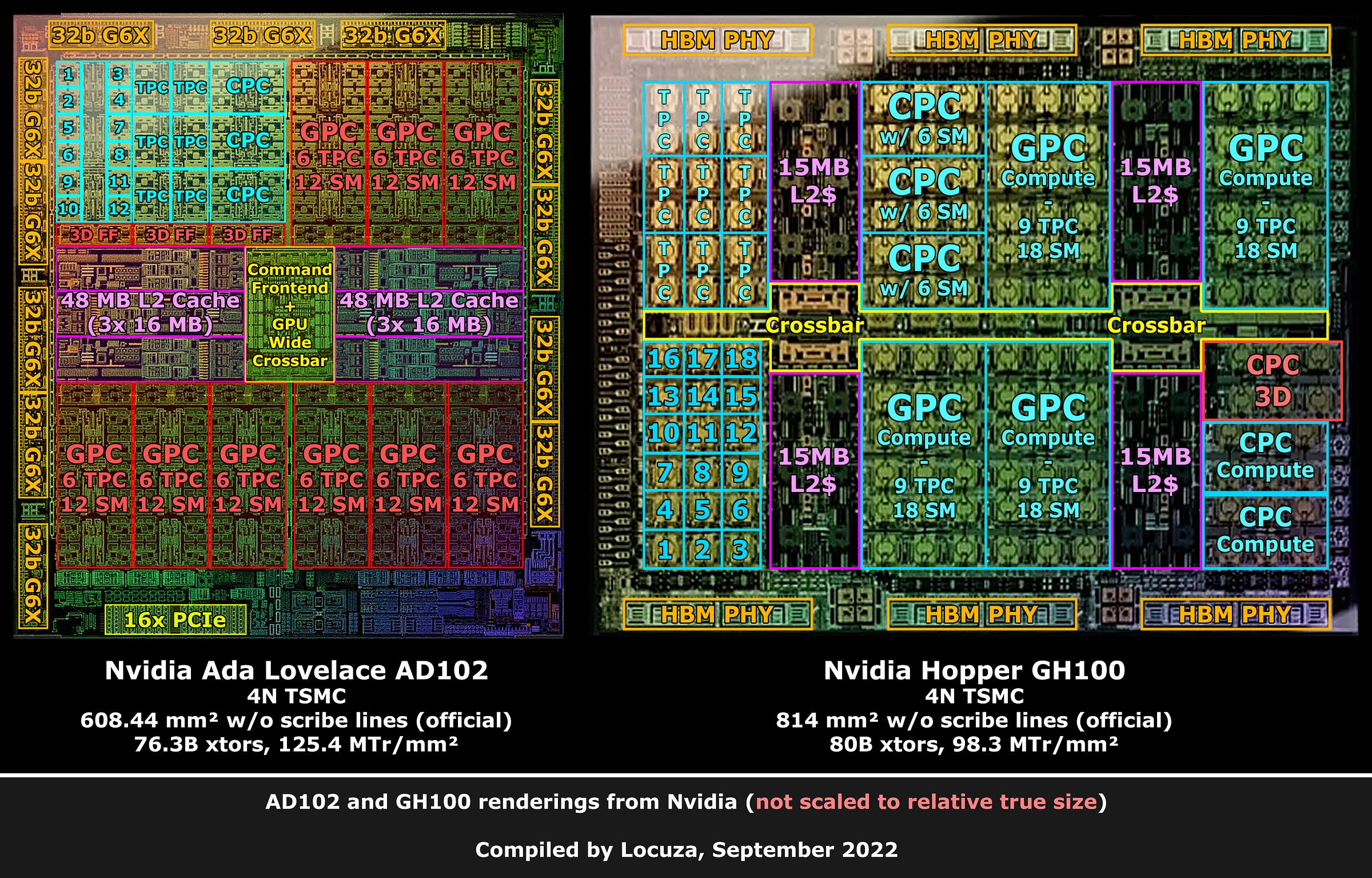
Nvidia did present an artistic die graphic for AD102, and unfortunately they go in the wrong direction with their images.
The previous rendering for Ampere GA102 was fairly close to reality, but now it’s again just some artsy depiction of the real chip.
But you know, I’m something of an artsy artist myself and also willing to suffer through other people’s delusions, I mean art.
So I’m running wild with my imagination and assume that AD102 is using the same package dimension of 51 mm x 51 mm as GA102 and takes around 618.33 mm² with the scribe lines (while conveniently ignoring the interesting looking package design).
Based on the official die size number, which is not including scribe lines, it appears to be a plausible size.
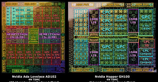
2.1 The simple AD102 floorplan interpretation next to the Hopper GH100 breakdown:
As the leaked software entries said, AD102 has in total 12 GPCs.
They are arranged as two rows, with the L2 cache, memory controlling and the command frontend between them.
The floorplan layout of HPC/AI Ampere and Hopper is quite different, as the L2 cache is split in two partitions (2x 24, respectively 2x 30 MB) with a hierarchical crossbar design.
When the Ada estimates were done, I wondered if AD102 will keep the GA102 design language or if Nvidia will follow the HPC line, as the increase in GPC count and L2 cache area might move the needle towards more localized interconnection.
For the 8 nm AD102 mockup I went with the GA102 design, as it already wired up even 7 GPCs in a row, where a 6+6 layout with a crossbar in the middle appeared like a suitable option.
One aspect I was curious about that isn't clearly visible at the top of the AD102 rendering is an NVLink PHY.
Ampere’s rendering did present a long PHY structure at the top (NVLink) and bottom (16x PCIe), sharing the same PHY design.
For Ada, we can’t find the same PHY stripe twice (for the top and bottom edge).
Furthermore, Nvidia did issue a press release for the upcoming workstation product RTX 6000 and doesn’t mention NVLINK once:
https://nvidianews.nvidia.com/news/nvidias-new-ada-lovelace-rtx-gpu-arrives-for-designers-and-creators
The predecessor did support it though:
https://www.nvidia.com/en-gb/design-visualization/rtx-a6000/
As such, the (old?) reference PCB design for Ada has likely an unnecessary NVLink connector, which can’t be utilized.
https://www.igorslab.de/en/ad102-and-ad104-why-there-is-no-real-information-yet-about-nvidias-new-geforce-cards/
Speaking of connections, Ada is “just” offering PCIe Gen 4 and doesn’t make the switch to 5.0 as Hopper did.
The DisplayPort standard also stays at 1.4a.
In the past, I was leaning towards the idea that Ada will utilize the same PCIe Gen5 IP as Hopper.
Now I’m curious if Ada is physically lacking PCIe 5 or if there is a similar situation as with the mobile Alder Lake chips, which physically have PCIe 5 integrated, but didn’t utilize it for cost measurements.
Die shots of AD102 and GH100 may give an answer, if we ever get both.
3.) Thanks to the Twitter feedback of August1 one architecture aspect cleared up.
Previously, I thought that PES could be analogous to what marketing calls a PolyMorph engine.
Since many years, Nvidia scales the PolyMorph engines with the amount of TPCs.
For the Ada diagrams, it was another point I was unsure about, as only 3 PES units per GPC were stated.
In the end I decided to draw the PolyMorph engines per TPC, which luckily was the right decision, as PES is (partly?) another hardware module, since TU102 also only has 3 per GPC.
Overall I’m expecting more than before, mostly the same 3D graphics pipeline.
On the flip side, I do wonder now if Ada Lovelace will introduce CPCs with a fast SM-to-SM network and Thread Block Cluster scheduling like Hopper or missing those concepts?
After all, the CUDA Compute Capability is stated to be 8.9 compared to 9.0 on Hopper.
It was 8.0 on GA100 and 8.6 on gaming Amperes.
Nvidia has an upcoming Q&A about various Ada related topics, and we should fairly soon get access to the whitepaper, that should clear up multiple questions.
::::::::::::::::::::::::::::::::::::::::::::::::::::::::::::::::::::::::::::::::::::::::::::::::::::::::::::::::::::::::::::::::::::::::::::::::::::::::::::::::::::::::::::::::
Subscribe for free to receive a newsletter when new content is available.
If you would like to support this work financially, you can choose the paid newsletter option or go to my Patreon page and select a tier that suits your budget - https://www.patreon.com/locuza


