Die analysis: Samsung Exynos 2200 with RDNA2 graphics
Part 1
Starting Info: This analysis was published on Patreon in April and is the first part of a planned two part series.
Part 2 lays half finished in the basement and I will get there sooner or later. :’)
For now, Part 1 shall also be online on Substack and serve as context.
::::::::::::::::::::::::::::::::::::::::::::::::::::::::::::::::::::::::::::::::::::::::::::::::::::::::::::::::::::::::::::::::::::::::::::::::::::::::::::::::::::::::::::::::

As a video on YouTube:
Samsung Exynos 2200 with RDNA2 graphics die shot analysis - Part 1
__________________________________________________________________________________
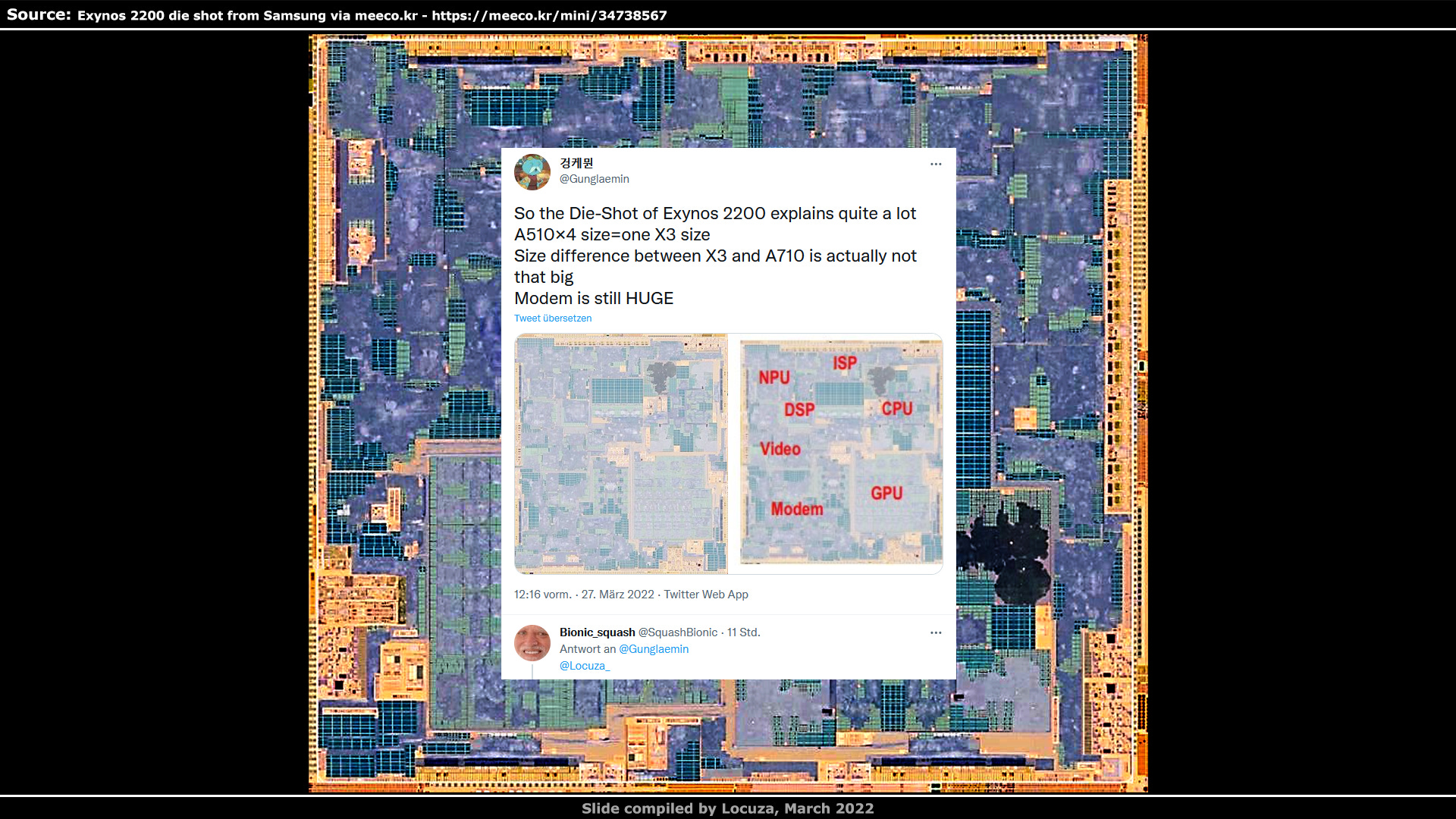
There it is, a die shot of the Exynos 2200, even shared by Samsung themselves!
A big thanks to Gunglaemin and Bionic_squash, who did find a source for the chip photo and made me aware of it.
I think there are a lot of people, who where excited to see how the next gen SoC of Samsung would fare with a custom GPU unit based on AMD’s RDNA2 IP.
The launch of that device was less than suboptimal and the initial impression looked not pretty.
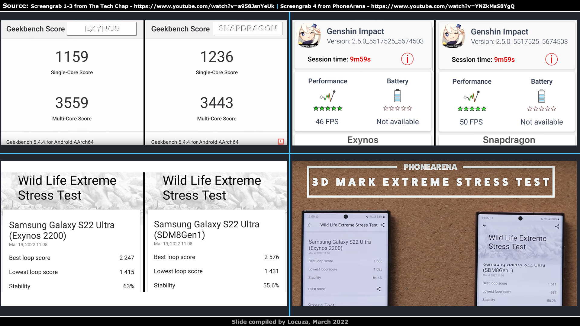
However, I recently searched for two reviews comparing the Exynos in the Galaxy S22 against the Snapdragon variant, and they seem to be fairly close together:
Screengrab 1-3 from The Tech Chap, showing CPU and GPU Exynos vs. Snapdragon results - https://www.youtube.com/watch?v=a958JsnYeUk
Screengrab 4 from PhoneArena, showing GPU Exynos vs. Snapdragon Wild Life Extreme results - https://www.youtube.com/watch?v=YNZkMsS8YgQ
The tests by The Tech Chap and PhoneArena were conducted in March using the newest system software at the time, where the CPU performance was basically the same, while on the GPU side the Snapdragon had the edge in terms of software support and performance.
But in regard to performance, the difference is primarily only at the beginning significant.
Under sustained load the advantage shrinks down to 10% or can go even below Samsung’s SoC.
Power efficiency is also very comparable, so overall the Exynos isn’t as far behind as feared, unless Samsung artificially equalized the energy consumption and performance between the devices.
And to be somewhat fair, Qualcomm has made a huge GPU jump with the latest Snapdragon chip and on AMD’s side it’s basically the first time that the GPU IP has been optimized to work well in a smartphone environment, excluding the mobile division Imageon that they had more than a decade ago and sold to Qualcomm.
Nonetheless, the goal was probably higher.
Rumors say that the implementation left a lot to be desired and that clock and efficiency targets were far from being met and that was Samsung’s fault.
I can’t judge how accurate the claims are, but if you want to read more about them or what in general is currently going wrong at Samsung, you can find a fitting article on SemiAnalysis, based on Korean sources:
https://semianalysis.substack.com/p/samsung-electronics-cultural-issues?s=r
That said, we will go through two topics in this series.
The first part will cover a floorplan walkthrough, detailing a few units.
Talking point number two will look at some structure sizes and a comparison with AMD’s desktop RDNA2 GPUs.
Before we begin, I have to bring up the usual disclaimer, I’m just a layman without any real expertise and I will make a lot of assumptions and potential mistakes, so don’t blindly trust anything I say.
Anyway..., let’s go. :)
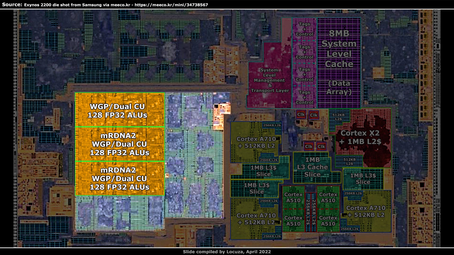
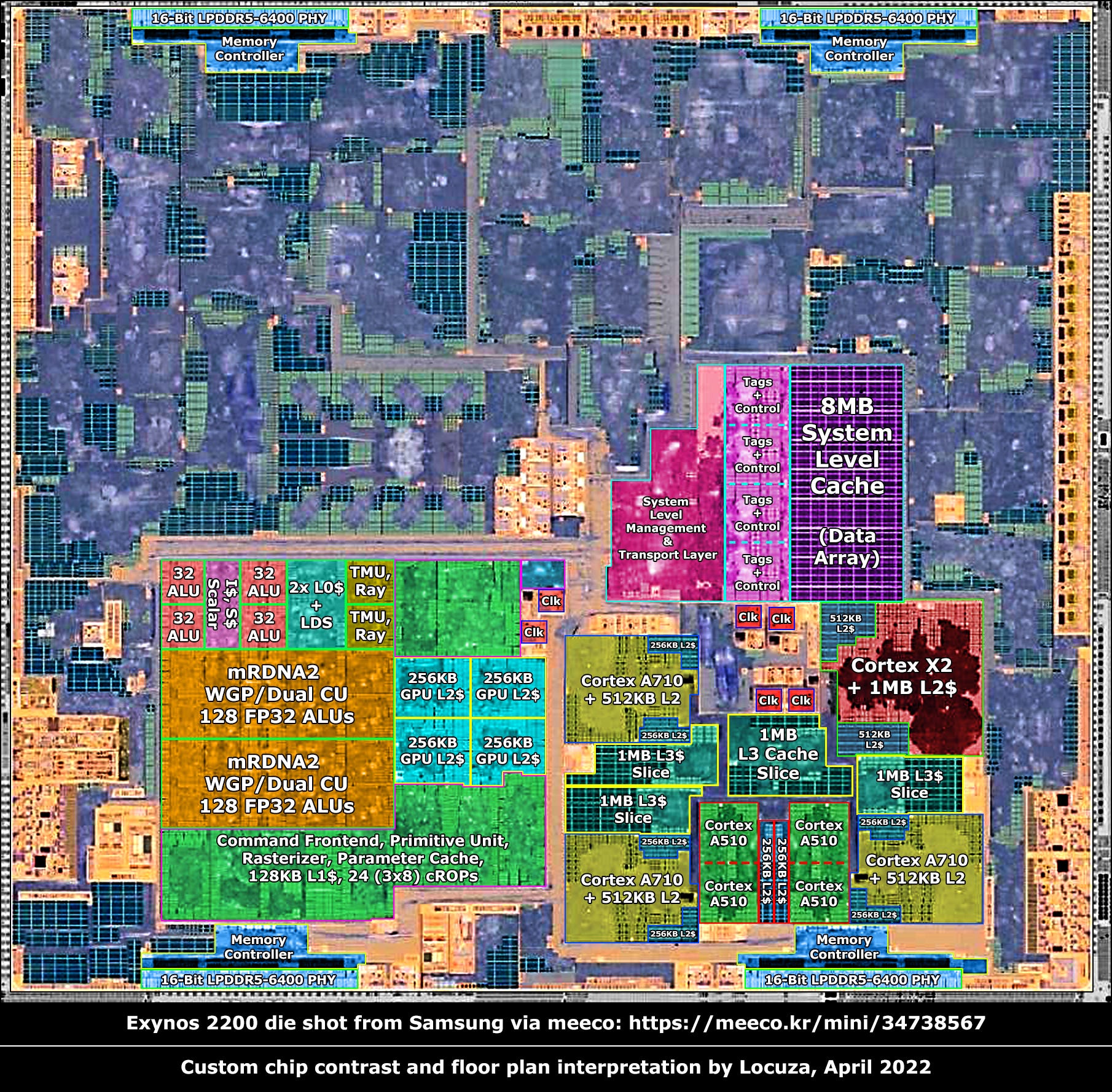
Samsung was so kind to tell us where 7 high-level elements are… roughly located.
That’s definitely better than nothing, but the chip has likely over 50 unique structures and over 100 subunits in total.
There is a lot of room to be more precise and at least for the CPU and GPU portion we will manage to present a finer picture, which in the best case is even correct.
As some may have noticed, I rotated the image to allow for a slightly larger zoom for the presentation, so don't get confused.
The CPU section is highlighted, and I won’t explain every little detail along the way, because a lot of it is just common knowledge, even for a layman.
Like remember back in kindergarten and how the teacher explained how SRAM cells are build and look like on a die shot, … yeah, things like that.
It always starts the same way as when we were four.
We look up the SoC specifications and hope that there is a somewhat useable documentation, to give us an idea what components are included.
In the best case, we can spot structures which correspond to a certain unit count and the high level-description.
For this chip, we know that inside the CPU area should be 8 CPU cores.
4 small and energy efficient Cortex-A510 cores that can be configured as a merged dual-core-cluster, sharing the floating-point unit and the L2 cache.
Some may be reminded of AMD's past Bulldozer design, which also shared those components between two integer cores.
However, they can also be laid down as separate single cores.
There are even more options, like the floating-point pipelines can be 64 or 128 bits wide and the L1 cache capacity can be configured to be either 32 KiB or 64.
It’s also possible to not use an L2 cache at all, or one with up to 512 KiB.
Quite a bit of low-level information here, but the only aspect which at first is important to us, is to look after four major structures which should be identical and represent the CPU cores.
In addition, the SoC uses three Cortex-A710 CPUs, which are much more beefy and use an out-of-order execution machine instead of in-order.
The L1 and L2 caches are also configurable, with the latter being able to store either 256 or 512 KiB.
Lastly, there is one Cortex-X2 core, which again is faster with a wider engine and deeper structures.
It’s there to provide the best single-threaded performance and fast response times.
Its L1 cache is always 64 KiB, and the L2 cache can hold 512 KiB or 1 MiB.
If we scan the CPU area for four identical structures, we can only find something like that at the bottom.
We do not see a clear separation line between all of those structures, and it looks like we have two dual-core clusters.
We can say with very high-confidence that those have to be the A510s, especially after we solved all other items.
The A710s are next, and it’s a simple matter, we clearly see three larger blocks, with no other available options.
Lastly, the Cortex-X2 is in the top-right corner.
That was easy, but we are not satisfied yet, are we?
So let’s figure out the L2 capacity at least.
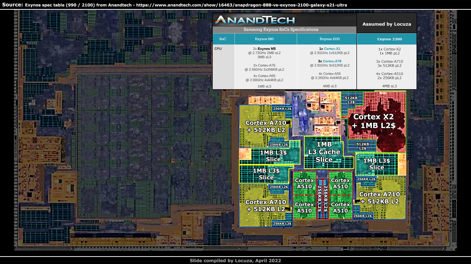
Samsung is not spilling the beans here, but we can look at the specs of the predecessor Exynos 2100.
That SoC used a very similar high-level configuration with three different core types.
The small cores used 64 KiB, while the A78s and the X1 used 512 KiB.
Qualcomm’s Snapdragon 888 utilized the same cores as the Exynos 2100, but equipped the small A55 cores with 128 KiB instead of 64.
Moreover, the X1 also got twice the capacity with 1 MiB instead of 512 KiB.
The Snapdragon 8 Gen 1 uses the same core setup as the Exynos 2200 with the same cache capacities as its Snapdragon precursor.
1 MiB for the prime core, 512 KiB for the mid-level cores, though for the small cores Qualcomm did not share the specs.
Now, while it does happen from time to time that a company reduces a cache size, from one generation to the next, there are usually good reasons for it.
With the Exynos 2200 it’s unlikely that Samsung reduced the capacity for the mid-level cores, from 512 KiB to 256, as there are no strong indications as to why this should have happened.
With high confidence, we can assume that the capacity is still at 512 KiB.
This means that the cores should have a fairly sizeable data array and simply based from a data flow and interconnection perspective, the L2 cache should be located at the edge of the complex.
Like here.
It’s physically split in two 256 KiB arrays, with the control logic in the middle.
This is often done for caches and other blocks to achieve shorter data paths with better latency and energy efficiency.
The SRAM macro tiles appear to store 16 KiB each.
When we turn our eyes to the Cortex-X2, it’s clear that the area taken by the L2 cache is much larger.
Although the image is quite blurry it looks like the SRAM tiles are the same and if we play a bit of Tetris with the A710 cache blocks we see that the area size is almost exactly double.
We can conclude that the Cortex-X2 is using a 1 MiB large L2 cache, as the Snapdragon 8 Gen 1.
With the A510 CPUs, it’s harder to figure out the storage size.
They use different SRAM cells and the pixel mess is a bit too hardcore for my liking, so let’s keep this a mystery for now or forever.
Up next is the L3 cache design, which is part of the DynamIQ Shared Unit 110.
The cache can be scaled in slices from 1 to 8.
A slice is segmented into roughly three parts.
An array of larger SRAM cells that store the data and have this visual check pattern (blue).
In addition, smaller SRAM cells are used for the cache tags, state information and parts of the snoop filter (green).
Furthermore, there is a control unit for the cache (purple).
I will spoil the capacity.
Based on measurements it can't be 2 MiB as that would result in a density far better than on Apple's N5 chips which are made by TSMC with currently the best density metrics.
On the other hand, 512 KiB would represent worse density than the L2 caches, so it has to be 1 MiB.
Now it gets funny, we can count the SRAM blocks, and it appears that we have 16 for one data array.
In total, we can find four of such structures, which are most likely the same, even though the piece in the middle has an interesting looking SRAM placement.
But the SRAM block between the A510 clusters is different.
Not only is it about half the size of the other cache slices, it also has a different check pattern, it looks like it’s using smaller and more SRAM blocks.
We could just ignore that detail and still assume 512 KiB.
Overall the L3 cache would be 4.5 MiB large and this doesn’t only sound strange, it’s also not possible according to Arm.
The cache slices have to be identical as multiple functions rely on that.
Moreover, Arm is saying that the slices are interconnected via a ring network and all other SoCs I have seen with a ring-based connection have a very straight alignment, which isn't the case here.
Something ain't right.
Perhaps the assumption is wrong that the L2 cache is part of the core area, and it’s actually located outside of it.
Visually, it also looks like the slices are laid down to be local per core.
This line of thoughts changes numerous aspects.
The L2 cache capacity for the A710 and X2 core would be the same at 512 KiB, as this is the only cache capacity which is possible under both cores.
Furthermore, each A510 dual-core cluster would have access to 128 KiB, effectively 64 per core and identical to the predecessor Exynos 2100.
After the L2 cache we obviously have to look for the L3 cache and there is a large data array right above the CPU cores.
It has apparently multiple identical slices and the alignment is nice and straight.
The check pattern is similar to the "CPU L2 caches" and from that we could assume that the total cache capacity is 4 MiB as on the predecessor.
Up to this point, this line of assumptions may seem more plausible in some respects, but it quickly breaks down in others.
It would be surprising to see the L3 cache that far away from the CPU cores, that wouldn’t be great for interconnection, latency and efficiency.
Further, beyond the L3 cache there should be a system level cache, which has been a standard for multiple SoC generations and there would be none on this chip, because there is no large SRAM array anymore which could be eligible.
It’s very doubtful that a system level cache isn’t used.
But the real kicker are area measurements.
If this supposed L3 cache has a capacity of 4 MiB, the density would be quite a bit worse than the cache design on AMD's 7 nm Zen3 CPU, given how little padding there is between the SRAM cells.
Zen3 is a high-performance CPU that can clock around 5 GHz and has to give something in terms of density.
That a mobile SoC in Samsung’s newest 4 nm node with high-density design cells and a clock target of 3 GHz would be worse off is not realistic.
In this regard, you might be surprised how much smaller RDNA2 is in the Exynos SoC, in comparison to the 7nm TSMC design.
So these cache capacities can’t be right.
Let’s go back to the initial starting point, which saw the L2 caches inside the core area.
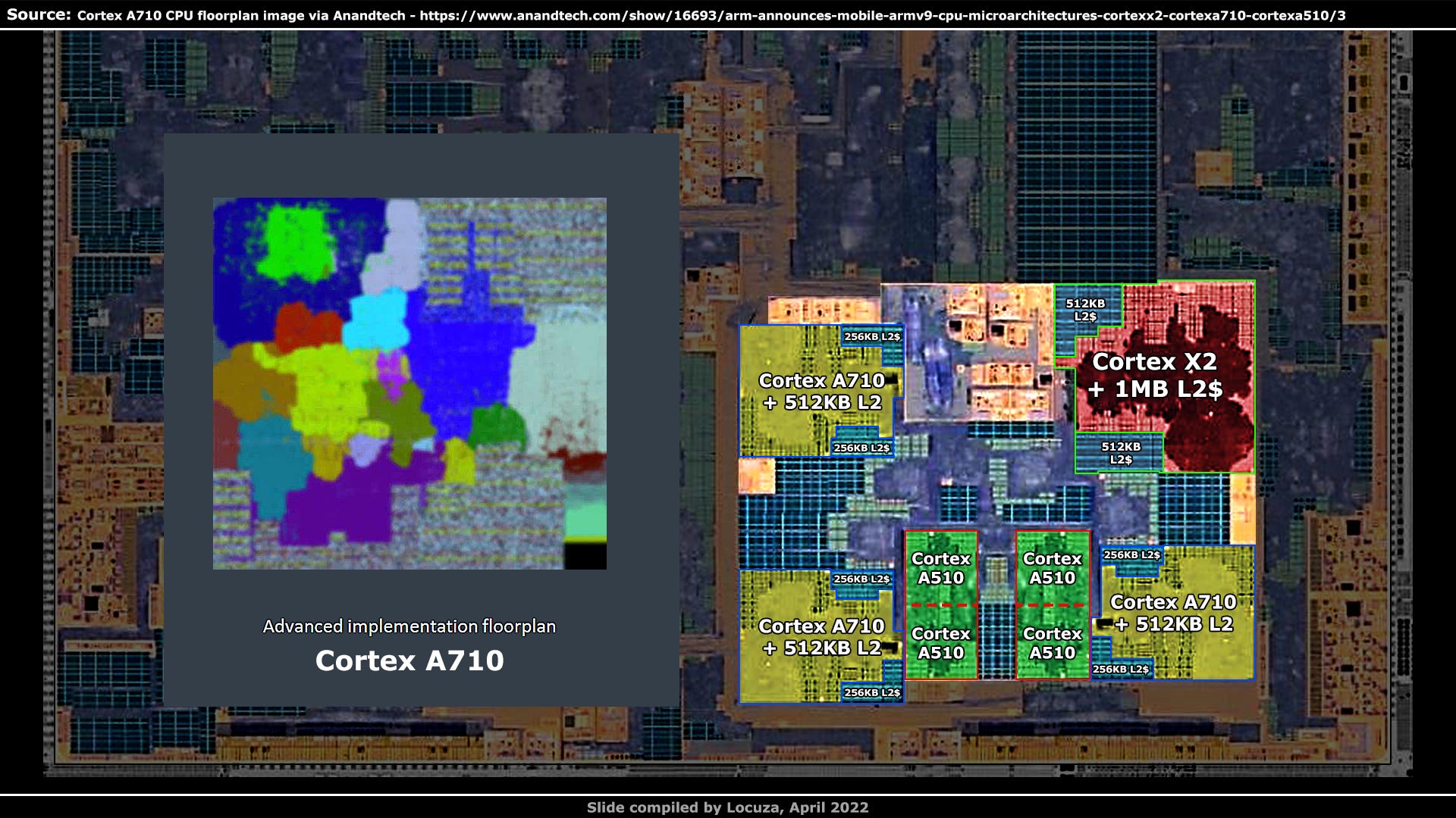
Arm is pretty good at sharing the core floor plan, and for the Neoverse-V1 it includes the L2 cache.
The core design is related to the Cortex-X1, but upgraded with a couple of HPC features.
It appears to be using 32 SRAM blocks at 32 KiB each and the same could be true for the larger Exynos CPU cores, depending on how it’s laid down.
There is also a floorplan for the Cortex-X2, that looks very similar to the V1 and is most likely also showing a 1 MiB L2 cache.
If you compare the floor plan to the Cortex-X2 on the Exynos SoC, you will notice that several changes were done, such as the SRAM placement.
The layout of the Cortex-A710 has also been modified and once again we see the same configuration as on the Exynos SoC, with a 512 KiB L2 cache.
From the current perspective, the cache slices outside the cores are for the L3 cache and hold 1 MiB each.
Besides the not so straight L3 cache alignment, our real problem child is the SRAM block between the A510 clusters.
We need to solve this issue to present a plausible picture.
So what does the floorplan for the A510 clusters show?
We see that Samsung has made the complex taller and less wide, but the SRAM cells are what we are looking for.
On the Exynos we have a roughly 50:50 or 40:60 split of SRAM blocks between the left and right side of the cores.
They are likely including the L1 caches.
Arm's design, on the other hand, does not show the same splitting and more SRAM cells on the right side.
Unfortunately, all images are fuzzy and don’t show the SRAM cells clearly, but I believe that the SRAM blocks on the right are for the L2 cache.
On the Exynos, the two clusters appear to be laid out in mirror symmetry, where we can make a clean cut between them.
The previous Arm images presented the maximum L2 cache capacity of the Cortex-X2 and A710, the same could apply to this A510 picture, but the Exynos is probably not using 512 KiB per cluster.
As mentioned before, the cache blocks likely store the same amount of data for a given area as the L3 cache cells, which would mean that per cluster 256 KiB are available.
All in all, this constellation is the one I believe most and so the assumed capacities are 1 MiB of L2 cache for the Cortex-X2, which is twice as much compared to its predecessor, which used 512 KiB.
The A710 cores use 512 KiB as the A78 cores before it.
As for the Cortex-X2, Samsung has also doubled the cache capacities per small efficiency core with on average 128 KiB instead of 64 KiB.
The shared L3 capacity remains the same, storing 4 MiB in total, which is less than the 6 MiB on the Snapdragon 8 Gen 1.
We are almost done with the CPU cluster by now.
The rest inside should contain various logic and interfaces for debugging, system level interconnection, a couple of power management units and clock generators, where 4 common ones are displayed at the top.
Further north is a huge array of SRAM.
We briefly glanced over it before.
It shows a similar check pattern and SRAM sizes as the CPU L3 caches, and based on that the capacity is probably 8 MiB.
Intuitively, one can assume that it’s the system level cache, which can be accessed by multiple clients.
Depending on the implementation, it’s possible to exclude some processing units, like the CPU, from the use of it or to limit the amount of cache which can be allocated by certain clients.
Based on benchmarks by Anandtech of the Exynos 2100, at least the CPU and GPU should utilize it.
The predecessor apparently also used 8 MiB for the system level cache.
That’s twice as much in comparison to the Snapdragon 8 Gen 1, which includes 4 MiB.
To the left, we can spot four repeating structures, with SRAM cells and digital logic.
The system level cache can likely be controlled as four slices.
Even further to the left is what I would suspect to be the system level control logic and the data transport layer.
This system level cache should primarily help the GPU performance and improve the efficiency, as more data can be fetched locally, instead of being pulled from external memory, where in Arm’s example there is a bandwidth reduction of 28%.
At long last, we are going to dissect the most interesting component of the SoC, the custom RDNA2 GPU.
Samsung and AMD announced in June 2019, that they would work together to integrate RDNA technology in the next generation products.
For around a decade Samsung was rumored to be working on its own GPU IP, which they cancelled at some point, to restart it later and to cancel it again and to maybe try it once more.
However, with the RDNA IP license, it’s clear that AMD is going to be the GPU provider for the foreseeable future, at least for high-end devices.
A switch from ARM's Mali IP that Samsung has been using for a very long time.
The issue with that technology is the competitiveness.
Apple’s and Qualcomm’s GPU technology enjoys a healthy lead in PPA, power, performance and area.
With AMD’s GPU design the goal was to be much more competitive and perhaps to elevate to the top.
In the past everything was unclear, we didn’t knew when chips with RDNA would come to market, with how many GPU Units and which RDNA variant would be integrated.
The recent press release talks about RDNA2 technology, but without further clarification this doesn’t mean too much, because the marketing folks have quite a lot of wiggle room, as seen with the Xbox Series and PS5 consoles.
According to the vendors, both are using RDNA2, but in reality they also utilize RDNA1 technology and the PlayStation 5 lacks Variable Rate Shading and likely dot-product instructions for AI applications.
But Samsung confirms two key features, that is support for hardware accelerated Ray Tracing and Variable Rate Shading.
With that, chances seem high that the full RDNA2 feature set is supported, in terms of basic functionality.
Beyond that, it’s possible that numerous customizations have been done, be it for power and clock management, some scaling attributes, possibly for certain memory capacities and perhaps even new features were added, like extra texture formats.
Before we look at the GPU silicon, allow me to present the last and most significant pieces of information.
The Korean site Gamma0burst looked at the firmware data and extracted gold for us tech enthusiasts.
First, the exact clock rates are unveiled for the CPU cores and their codenames.
While Klein and Matterhorn were known and reported by the media, no codename was given for the Cortex X2, but now we know it's Montblanc.
Well not now, the webpage is online since March, but for me it’s new, and I hope for some others too.
The clock speeds align with what was stated by the media, with the exception of the small A510 cores, their clock rate was said to be 1.7 GHz, instead of the listed 1.824.
The GPU clock range is 303 MHz up to 1.306 GHz.
That’s nearly half the clock speed of Navi22 in the 6700 XT.
But not so far off in comparison to the Steam Deck, which clocks up to 1.6 GHz, or the 6300M, with an official clock rating of 1.5 GHz.
It was claimed by Ice Universe that the initial peak target was 1.9 GHz, which later had to be adjusted to 1.7, to 1.5 and finally down to 1.3 GHz, due to thermal and efficiency issues.
I’m not sure if the initial target was really that high, but the peak clocks are not so interesting anyway.
I’m more curious about how the sustained average clock went down.
Qualcomm says the Adreno 730 in the Snapdragon 8 Gen 1 can clock over 800 MHz, so the peak clock would be 60% higher on the RDNA2 GPU, but what is actually achieved in applications is another story.
Then there are the following nuggets.
MGFX0 is the Xclipse 920 found in the Exynos 2200, but there is also another GPU unit called the Xclipse 930.
Furthermore, in the code MGFX0 and 1 are abbreviated as M0 and M1.
Another fascinating point is that the codename for AMD’s IP is Van Gogh Lite.
Van Gogh is the codename for the SoC found in the Steam Deck, but this doesn’t mean they are related in any way, beyond the namesake.
The interesting point for me is that Van Gogh Lite has an entry with M0 and M1, potentially leading to the assumption that Samsung will have two different GPU configurations, with the 930 coming later.
Eventually we get a configuration table for M0 and M1, stating what is behind those GPUs and every entry is just bliss in the eyes of the tech-fetish.
At the very beginning, the Graphics Core IP version is said to 10.4, which is higher than on any other RDNA2 GPU.
3 WGPs are found on M0, or 6 Compute Units, that’s something which the rumor mill spilled a long time ago for the Exynos 2200, this entry would simply confirm it.
The next line came as a semi-surprise to me because I read it after finishing the annotations where I was wondering about this point.
It most likely talks about 3 render backends per shader array.
If the standard RDNA2 configuration is used, that would mean 24 ROPs, more than what the pixel frontend can deliver.
The scan converter has 2 packers as on Van Gogh and RDNA1 GPUs, so most likely 16 pixels per clock are rasterized.
One assumption might be that one render backend is extra to improve the yield, but this would cost quite a bit of extra area and lead to the question if we are looking at the active GPU configuration or at what is physically present?
Config mode M0 sounds more like the active setup.
It becomes confusing with M1 because the graphics core version is changed to 40_1.
Maybe it’s just a placeholder or a typo, the graphics core version should not change if we are talking about the same chip.
The only difference in comparison to the M0 is the amount of WGPs, instead of 3 there are 4, as on the Steam Deck.
So if it's just a software defined GPU mode, we should physically see 4 WGPs on the die shot and the Exynos 2200 would be using a stripped down chip configuration.
But this is not the case, physically just 3 WGPs are present and M1 needs to be another chip.
I find it surprising that both chips are codenamed Van Gogh Lite.
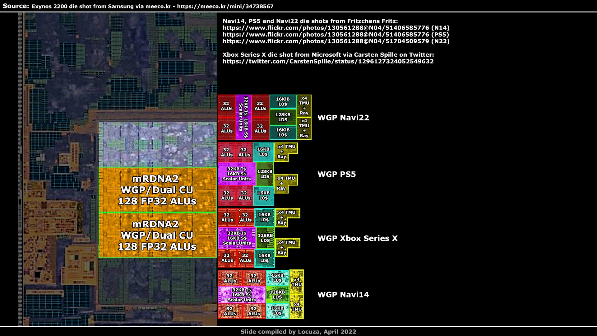
The WGPs are easy to identify, since we have many RDNA die shots from Fritzchens Fritz and we already know how the basic floor plan looks like.
All displayed WGPs share a common design language, but have differences in terms of SRAM placement and the width and height of the building blocks.
I will keep it short this time.
Each SIMD unit has 128 KiB for the vector register file, this register file is made out of SRAM cells.
Visually we see exactly four units, which have the same amount of SRAM cells.
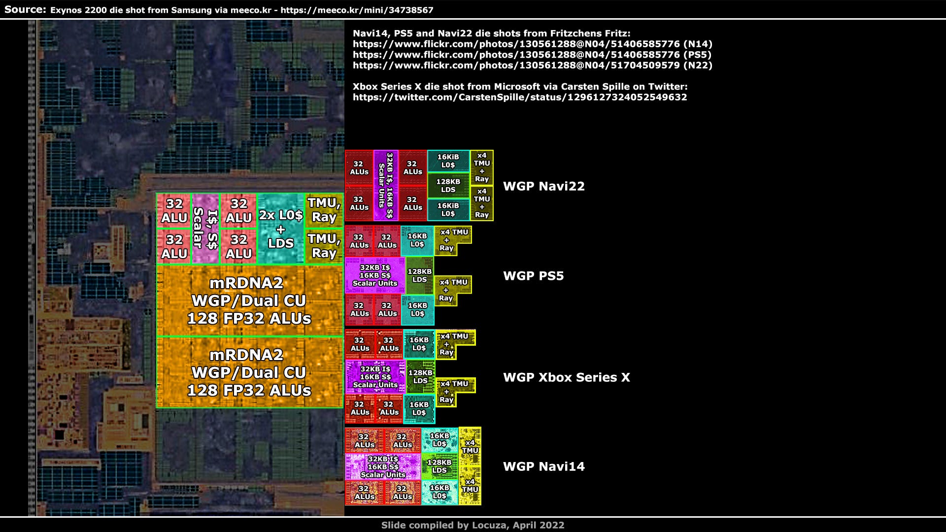
Once you know how much data one cell is storing, you can look for the same cells in other blocks and, for example, make an educated guess as to where the instruction and scalar cache is likely located.
In addition, there should be logic which includes the scalar units, their scalar register file and perhaps also the compute frontend.
Based on proximity, these components are most likely between the SIMD units.
Here we see a larger floor plan difference between Navi22 and all others.
While the rest has SIMD units at the top and bottom, which are separated by logic blocks along the horizontal axis, Navi22 places the SIMD units on the left and right side, separating them with vertically stacked logic.
The local data share is easy to find as the capacity is large with 128 KiB and it only exists one time.
One can also count 32 or 64 SRAM blocks, numbers which fit to the 128 KiB capacity.
Close to the LDS we should find two texture mapping units and two 16 KiB L0 caches.
What is inside the cyan blocks is not exactly what you would expect for the L0 caches since the SRAM count leads to 24 KiB.
But the other blocks look less likely to me, as they even store 32 KiB and contain many different SRAM cells.
Based on previous GPU designs, I’m more inclined to believe that the texture mapping units, load/store and ray tracing accelerators are at the edge of the WGP.
How does the mobile RDNA2 WGP in the Exynos looks like in comparison?
It looks blurry, disgustingly blurry.
That aside, to me, it looks more like the Navi22 layout design with less symmetrical SRAM placement.
I would love to see a more defined image, as the LDS is harder to make out and doesn’t appear to be located in the center as previously.
Moreover, if the basic floor plan is the same, the TMUs have grown significantly in size.
After the WGPs, the GPU L2 cache might be relatively easy to find, as we should see multiple blocks with a larger amount of SRAM cells.
AMD’s GPU designs usually have one L2 cache tile per memory channel, but it’s possible to have more or less.
But first, how many memory channels are there on the SoC?
According to the press, 64 bits are used for the LPDDR5 interface.
A memory channel is 16 bits wide under LP5 memory, so we should see 4 I/O PHYs or repeating segments.
Once again it turns out to be simple as only these structures do appear 4 times.
At the edge is the physical layer to the LP5 memory, which runs at 6.4 gigabits per second.
Above or below the PHY is digital control logic for the memory operations.
Currently, we can expect to see 4 L2 cache tiles on the GPU, one per memory controller/channel.
The pixel smearing doesn't make it easy, but on the right side we have a large collection of SRAM cells.
It looks like we can split them into about 4 equal slices, where on the right side of each block we have the data arrays.
This matches the L2 cache design on other RDNA GPUs from AMD.
Obviously we are curious about the capacity per tile.
For recent GPU designs, AMD uses 256 KiB, but perhaps they cut it down, or maybe they even use 512 KiB as on Rembrandt, to keep more data local.
Compared to Navi22 and the CPU L3 cache, the size proportions indicate that the capacity is probably 256 KiB, definitely not 128 KiB.
The rest is harder to break down.
At the bottom center is a dense SRAM array, likely for the parameter cache.
To the right could be two Render Backends, each consisting of a color ROP block and a depth ROP block.
However, the relative size would be a lot larger than on Navi22.
In general, I would simply state that inside the green area should be the command frontend, the geometry engine, a rasterizer, the parameter cache, 128 KiB of L1 cache for the shader array, and 24 color ROPs plus depth ROPs.
The small logic block in the upper right corner has a different color tone.
One assumption could be that it’s an interface block that manages data transfers between the GPU and the system level cache.
Or maybe it has more to do with power functions, as there are multiple analog devices and two clock generators below it.
That’s it for now, an update with the rest will follow later. :)
_______________
Sources in chronological order:
https://docs.google.com/document/d/1gIHtLB6PCXf61KC_hrcZtnJC1R9-8rB7FR2-MQZ6094/edit?usp=sharin
____________________________________________________________________________________________
Subscribe for free to receive a newsletter when new content is available.
If you would like to support this work financially, you can choose the paid newsletter option or go to my Patreon page and select a tier that suits your budget - https://www.patreon.com/locuza


